Optimal mosfet driver circuit for reducing electromagnetic interference and noise

a driver circuit and electromagnetic interference technology, applied in electronic switching, pulse technique, semiconductor devices, etc., can solve the problems of increasing the power loss of the circuit, reducing the power conversion efficiency, and ringing, so as to reduce the dead time and power consumption, and the effect of reducing the spike of voltage and curren

Inactive Publication Date: 2011-11-10
SEMTECH CORP
View PDF5 Cites 8 Cited by
  • Summary
  • Abstract
  • Description
  • Claims
  • Application Information

AI Technical Summary

Benefits of technology

[0008]Embodiments of the present invention are directed to controlling the turn-on and turn-off profiles of the primary switching FET assembly of a power converter in order to minimize voltage and current spikes while also reducing dead time and power consumption.
[0010]An embodiment of the present invention further includes a control circuit that controls the fast shunt circuit and the slow shunt circuit in order to control the turn-off profile of the primary FET switching assembly. In one embodiment, the control circuit closes the fast shunt circuit and the slow shunt circuit during a first time interval such that the primary switching FET is driven rapidly toward an off state. During a second time interval, the fast shunt switch is opened such that the primary switching FET is driven more slowly toward the off state, and during a third time interval, the fast shunt switch is closed again to drive the primary FET the rest of the way off at a rapid rate. The time intervals are adjusted to reduce voltage and current switching spikes while at the same time to reduce power consumption and dead time.

Problems solved by technology

In a switching power converter, it is known in the art that parasitic inductances and capacitances of circuit elements can produce resonances that result in large voltage spikes and ringing when the primary MOSFET is switched off.
These voltage spikes can lead to avalanche breakdown of the MOSFET insulator, eventually damaging it.
A disadvantage of using a snubbing circuit is that it increases the power loss of the circuit and thus reduces the power conversion efficiency as power is dissipated in the snubber diode and resistor.
In addition, the snubber necessarily slows the turn-off time of the MOSFET.
In a high-frequency power converter, this can introduce significant dead time, dramatically reducing system efficiency.

Method used


Image

  • Optimal mosfet driver circuit for reducing electromagnetic interference and noise
  • Optimal mosfet driver circuit for reducing electromagnetic interference and noise
  • Optimal mosfet driver circuit for reducing electromagnetic interference and noise

Examples


Embodiment Construction

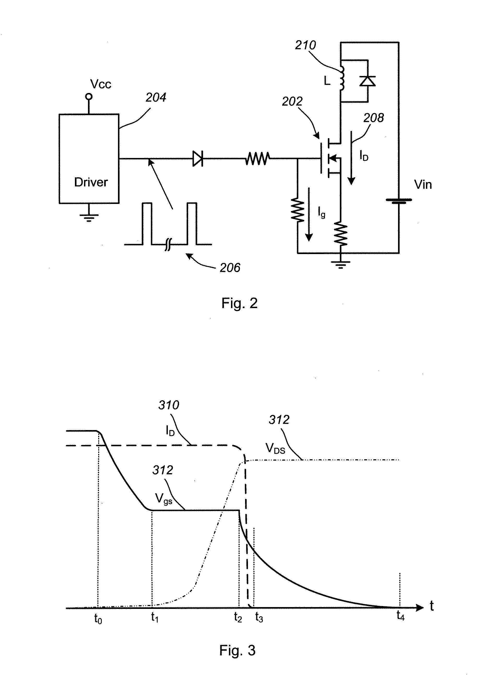
[0026]An embodiment of present invention controls the turn-off profile of a MOSFET or similar device in order to reduce voltage spikes and electromagnetic interference (EMI) while at the same time limiting power losses and retaining relatively fast switching speeds. For example, the table below compares three simulations of a 30-Volt MOSFET switching circuit. Case one shows a fast turn off of a MOSFET in a circuit with no snubber. Case two shows a slow turn off for a circuit in which a snubber typical of the prior art is used. Case three shows a controlled MOSFET turn off in a circuit in accordance with an embodiment of the present invention.

Case 1Case 2Case 3NoTypicalEmbodiment of thesnubbersnubberpresent inventionSpike (V)51V31V31.5VSwitching power1.61W3.1W2.3Wloss (W)Switching time (ns)22.7ns186ns50ns

[0027]As can be seen from the table above, the use of a snubber can significantly reduce the magnitude of the voltage spike from 51 V to 31 V. However, it also increases the switchin...


PUM


Abstract

A system and method of controlling the primary switching FET turn-on and turn-off profiles in a switching power converter suppresses voltage and current spikes, reduces power consumption, and reduces system switching time. A combination of fast and slow shunt circuits is used to control current flow through the primary switching FET. The FET switching rate is slowed during the period of maximum current change to limit the magnitude of switching spikes and is allowed to proceed rapidly at other times to reduce switching time and power consumption.

Description

RELATED APPLICATION DATA[0001]This application claims priority pursuant to 35 U.S.C. §119(e) to U.S. provisional patent application Ser. No. 61 / 331,156, filed May 4, 2010, the subject matter of which is incorporated by reference herein in its entirety.BACKGROUND OF THE INVENTION[0002]1. Field of the Invention[0003]The invention relates generally to the field of switching power converters, and more particularly, to drive circuits for MOSFETs that minimize switching power loss while simultaneously reducing switching time and improving system efficiency.[0004]2. Description of Related Art[0005]In a switching power converter, it is known in the art that parasitic inductances and capacitances of circuit elements can produce resonances that result in large voltage spikes and ringing when the primary MOSFET is switched off. These voltage spikes can lead to avalanche breakdown of the MOSFET insulator, eventually damaging it. It is therefore necessary to reduce the magnitude of these voltage...

Claims


Application Information

Patent Timeline
Patent Type & Authority Applications(United States)
IPC IPC(8): H03K17/04
CPCH03K17/163H03K17/04106
Inventor LIN, FENGCHANG, CHIN
Owner SEMTECH CORP
Why Eureka
Try Eureka