Method for manufacturing monolithic ceramic electronic component, and multilayer composite

a technology of monolithic ceramic and electronic components, which is applied in the direction of soldering apparatus, transformers/inductance coils/windings/connections, magnetic bodies, etc., can solve the problems that the industry element may not exhibit desired characteristics, and achieve the reduction of the inflection point of the magnetic field, the effect of reducing the manufacturing cost of the monolithic ceramic electronic component and facilitating plurality of turns

Inactive Publication Date: 2007-08-09
MURATA MFG CO LTD
View PDF11 Cites 20 Cited by
  • Summary
  • Abstract
  • Description
  • Claims
  • Application Information

AI Technical Summary

Benefits of technology

[0024] In order to form the multilayer composite in preferred embodiments of the present invention, the following steps are performed: forming a first conductor pattern for a portion of the coil conductor on a first main surface of a first ceramic green sheet, a second conductor pattern intended for the another portion of the coil conductor on a first main surface of a second ceramic green sheet, and stacking the first ceramic green sheet and the second ceramic green sheet such that the first main surface of the first ceramic green sheet opposes the first main surface of the second ceramic green sheet with the core therebetween, and such that the ends of the first conductor pattern come into contact with the ends of the second conductor pattern to form a conductor in a coil form. With these steps, the conductor having a coil shape can be provided without forming a via hole conductor in a specific ceramic green sheet. Accordingly, the step of forming a via hole conductor is not required, and thus, the manufacturing cost of the monolithic ceramic electronic component is reduced.
[0025] When a multilayer composite is formed as described above, the coil conductor formed around the core is in close contact with the core, such that the magnetic flux generated is completely confined and the inflection point of the magnetic field is reduced. Thus, a low-loss inductor element is provided.
[0026] In the above-described preferred embodiment, if each of the first and second conductor patterns each has a plurality of conductive strips, the resulting coil conductor can easily have a plurality of turns. In this instance, the pitch of the plurality of conductive strips can be reduced without limitations on the size of the via hole conductor. If the conductive strips are formed by screen printing, the pitch of the conductive strips depends on only the printing characteristics of screen printing, and can be reduced to, for example, about 30 μm. Accordingly, the size of the coil conductor, and thus the size of the monolithic ceramic electronic component, can be reduced.
[0027] In the formation of the multilayer composite according to the above-described preferred embodiment, if the step of stacking the first ceramic green sheet and the second ceramic green sheet is performed by disposing the core on the first main surface of the first ceramic green sheet such that the ends of the first conductor pattern protrude from the core, and then by stacking the second ceramic green sheet on the first ceramic green sheet with the core therebetween, the multilayer composite is formed by stacking its members one after another from one side in the stacking direction. Thus, the multilayer composite can be prepared without using a complicated process.
[0028] In preferred embodiments of the present invention, if the multilayer composite further includes first shield plates made of a magnetic ceramic sintered compact along specific interfaces of the ceramic green sheets such that the core and the coil conductor are disposed between the first shield plates in the stacking direction, the first shield plates and the shrinkage restraining layer prevent shrinkage in the firing step. In addition, the lines of magnetic force can be confined to run from the inductor element including the core and the coil conductor in the stacking direction. Consequently, elements disposed around the inductor element which are readily affected by the magnetic field, such as a transformer, are shielded, and the loss is reduced.
[0029] If the multilayer composite further includes second shield plates made of a magnetic ceramic sintered compact at the interface of the green ceramic layers between which the core and the coil conductor are disposed, such that the core and the coil conductor are disposed between the second shield plates, the confinement of the lines of magnetic field is further improved, and the loss of the inductor element is further reduced.

Problems solved by technology

For example, the inductor element may not exhibit desired characteristics in the resulting monolithic ceramic electronic component.

Method used


Image

  • Method for manufacturing monolithic ceramic electronic component, and multilayer composite
  • Method for manufacturing monolithic ceramic electronic component, and multilayer composite
  • Method for manufacturing monolithic ceramic electronic component, and multilayer composite

Examples


Embodiment Construction

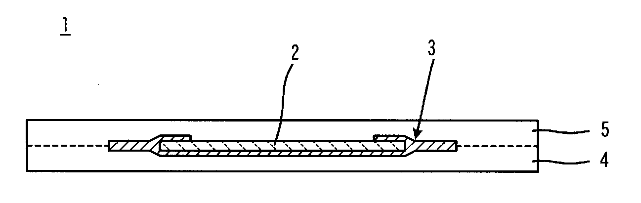
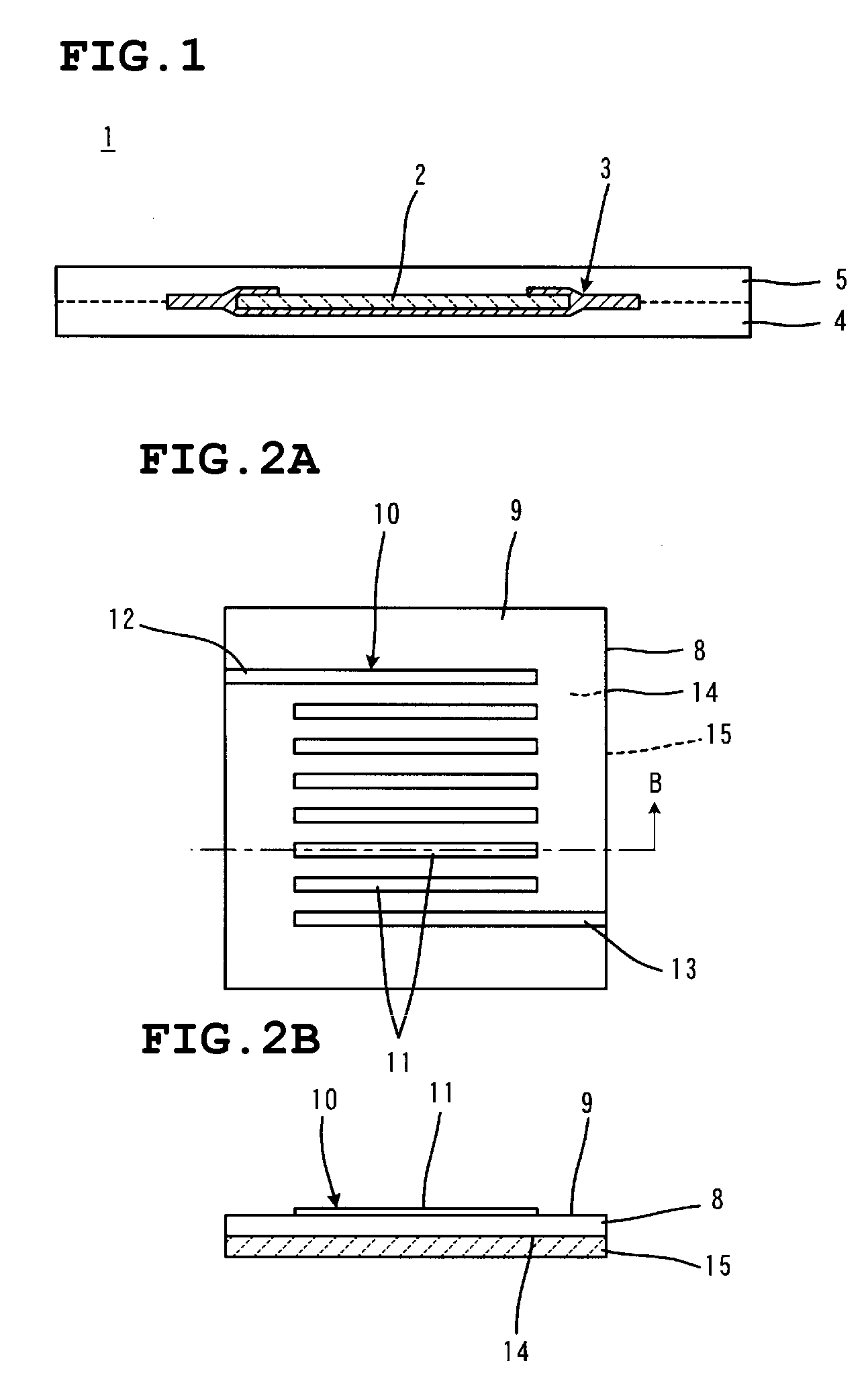
[0050]FIG. 1 is a sectional view of an inductor element 1 according to a first preferred embodiment of the monolithic ceramic electronic component manufactured by a manufacturing method of the present invention.

[0051] Referring to FIG. 1, the inductor element 1 includes a core 2 made of a sintered compact of magnetic ceramic, such as ferrite, a coil conductor 3 disposed around the core 2, and two ceramic layers 4 and 5 between which the core 2 and the coil conductor 3 are disposed. The inductor element 1 is manufactured by a method described with reference to FIGS. 2A to 5B.

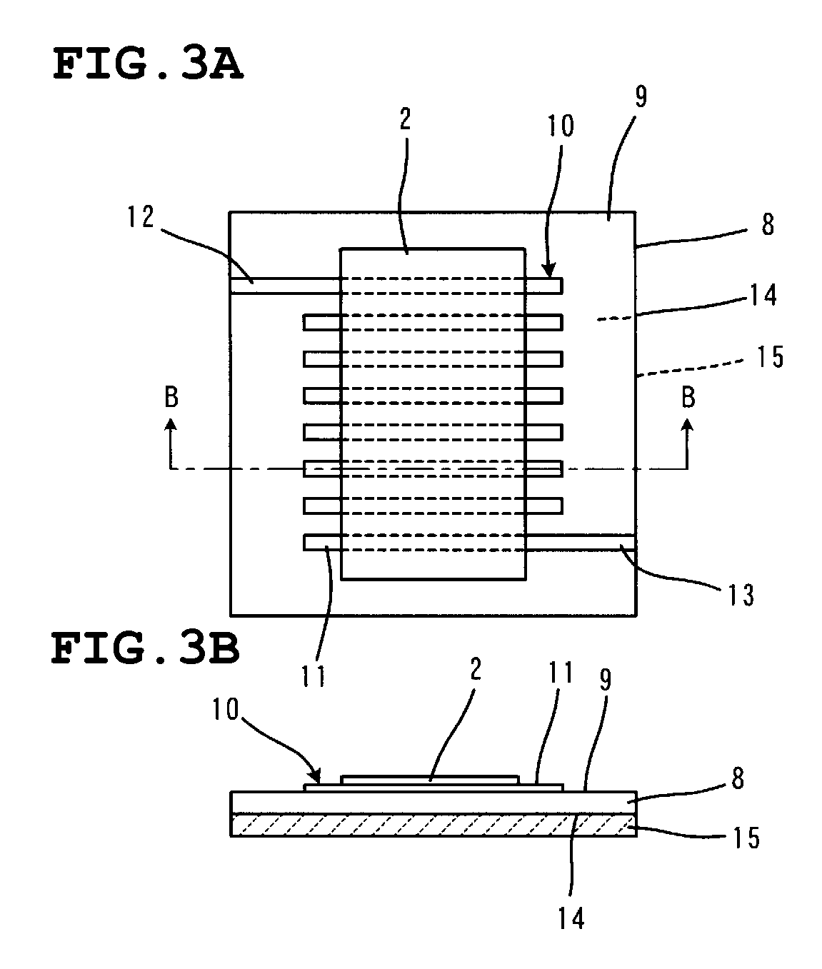
[0052] In each of FIGS. 2A to 5B, A is a plan view and B is a sectional view taken along line B-B of the respective plan view A.

[0053] Referring first to FIGS. 2A and 2B, a first ceramic green sheet 8 for the ceramic layer 4 is prepared. Preferably, the first ceramic green sheet 8 primarily includes a low-temperature co-fired ceramic material. For example, the first ceramic green sheet 8 is formed in a sheet b...


PUM

PropertyMeasurementUnit
thicknessaaaaaaaaaa
pressureaaaaaaaaaa
pressureaaaaaaaaaa

Abstract

A multilayer composite including a core made of a magnetic ceramic sintered compact disposed therein, and shrinkage restraining layers including an inorganic powder that is not substantially sintered at the sintering temperature of the green ceramic layers are sintered in order to reduce the difference in shrinkage behavior during firing between the core and the green ceramic layers.

Description

BACKGROUND OF THE INVENTION [0001] 1. Field of the Invention [0002] The present invention relates to a method for manufacturing a monolithic ceramic electronic component including a coil conductor, and a multilayer composite prepared for manufacturing the monolithic ceramic electronic component. [0003] 2. Description of the Related Art [0004] Monolithic ceramic electronic components including an inductor element as disclosed in Japanese Unexamined Patent Application Publication Nos. 11-260642 (Patent Document 1) and 2000-150239 (Patent Document 2) are related to the present invention. In order to manufacture a monolithic ceramic electronic component including an inductor element, Patent Documents 1 and 2 disclose a process including the step of preparing a green stack including a green core primarily including a green magnetic material, a coil conductor made of a green electroconductive paste film around the green core, and green outer layers primarily including a green non-magnetic...

Claims


Application Information

Patent Timeline
Patent Type & Authority Applications(United States)
IPC IPC(8): H01F5/00
CPCH01F17/0013H01F41/046H05K1/0306H05K1/165H05K3/4611H05K3/4629Y10T29/49069H05K2201/09763H05K2203/308Y10T29/49144Y10T29/4902Y10T29/49071Y10T29/49073H05K2201/086
Inventor WADA, RYUICHIROIKEDA, TETSUYA
Owner MURATA MFG CO LTD
Why Eureka
Try Eureka