Component mounting method and component mounting apparatus

a technology for mounting components and components, applied in the direction of sustainable manufacturing/processing, final product manufacturing, cooking vessels, etc., can solve the problems of inability to deal with fine-pitch chips that require high positional precision, inability to tolerate, etc., to reduce the effect of thermal expansion, suppress heat conduction, and increase joint resistance and bonding failur

Inactive Publication Date: 2007-08-09
PANASONIC CORP
View PDF5 Cites 26 Cited by
  • Summary
  • Abstract
  • Description
  • Claims
  • Application Information

AI Technical Summary

Benefits of technology

[0015] With this first component mounting method, the placement head is lowered to press the electronic component onto the substrate until a preset contact load is detected, and so even if the electronic component has lost its flatness because of undulation or warping due to the suction, it is corrected to have a desired flatness as it is pressed with a flat suction surface of the suction nozzle, and therefore bonding failures that may result from deformation of IC chips are prevented. IC chips, which are one example of electronic components, tend to be made thinner, and they include a multiplicity of fine-pitch electrodes due to high integration technologies; if they are not completely flat, all the electrodes may not be uniformly bonded to the substrate electrodes. With this component mounting method, even electronic components that are thin and can easily lose their flatness are mounted with good bonding conditions.
[0035] In any of the above apparatuses, it is preferable to provide a heat insulating member having a thermal expansion coefficient of not more than 1×10⁻⁶ between the placement head main body and heating means that is interposed between the suction nozzle and the placement head main body. This suppresses heat conduction from the heating means to the placement head body, and mitigates effects of thermal expansion.

Problems solved by technology

The problem was that this method could not deal with fine-pitch chips that require high positional precision and cannot tolerate the slight misalignment in the bonding positions that may occur when air is blown to break vacuum to release the chip.

Method used


Image

  • Component mounting method and component mounting apparatus
  • Component mounting method and component mounting apparatus
  • Component mounting method and component mounting apparatus

Examples


Embodiment Construction

[0046] The following embodiment of the invention is a component mounting method and a component mounting apparatus for mounting IC chips on a substrate, the IC chips being one example of electronic components and having solder bumps as protruded electrodes, which are fused to pads on the substrate (substrate electrodes). More particularly, a method and apparatus for controlling the mounting operations is provided, which enables precise mounting of thin IC chips that tend to lose their flatness, or fine-pitch and high-pin-count IC chips. Target object on which IC chips are mounted is a substrate here, but it may not necessarily be a circuit substrate but an IC chip, e.g., in the case with “chip-on-chip”, in which an IC chip is mounted on another IC chip.

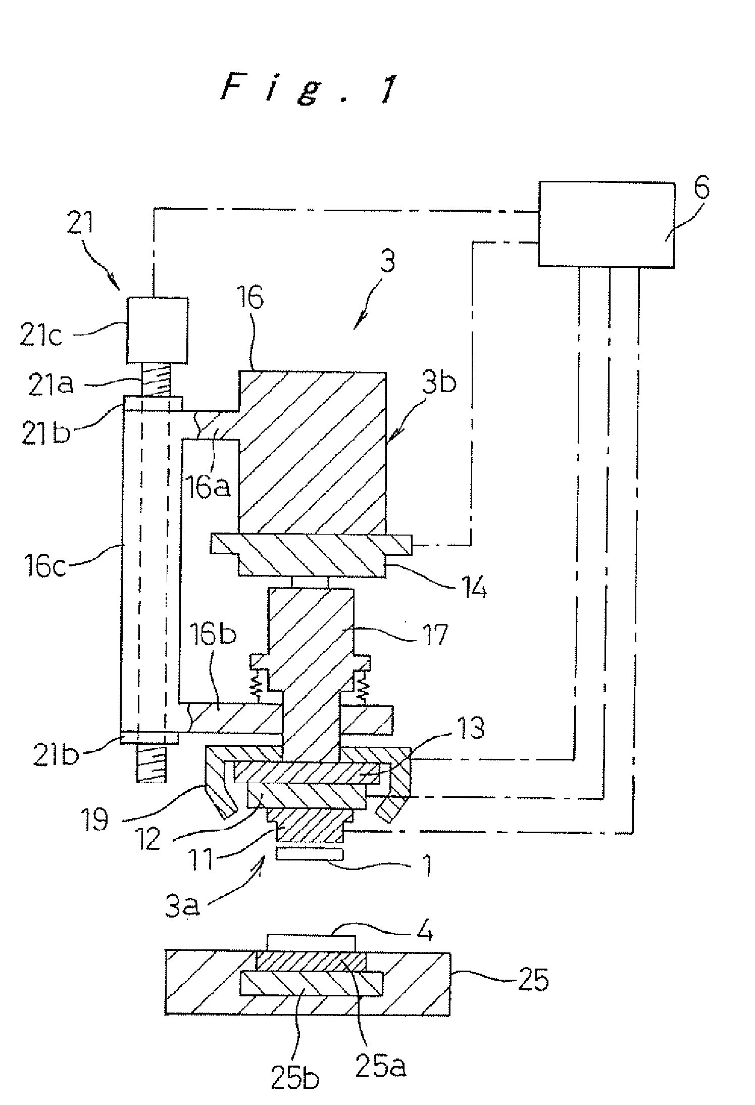
[0047]FIG. 1 illustrates the main features of one embodiment of the mounting apparatus; the drawing shows the part of a placement head 3 where an IC chip 1 is held with a suction nozzle 11 to be mounted on a substrate 4 held on a mou...


PUM


Abstract

A method and an apparatus for mounting electronic components that enables precise mounting of electronic components, such as deformation-prone thin IC chips or fine-pitch and high-pin-count IC chips, on a substrate. Thin IC chips, which conventionally tend to lose flatness because of warping that occurs during production or deformation that occurs when picked up with a suction nozzle, are pressed against a substrate (4) with a preset load using a suction nozzle with a flat suction surface (11b) so as to correct deformation; the suction nozzle (11) is controlled to move up to make up for a decrease in the distance between the oppositely spaced IC chip and the substrate (4) that is caused by thermal expansion due to the heating for melting solder bumps (1a) on the electrodes; and the suction nozzle (11) is controlled to move down to mitigate the effect of a pulling-apart force applied to the molten parts as the thermally expanded parts cool down and contract.

Description

TECHNICAL FIELD [0001] The present invention relates to a method and an apparatus for mounting electronic components on a substrate which is a target object using flip-chip mounting techniques, and in particular to a component mounting method and a component mounting apparatus which enable precise mounting of electronic components such as thin IC chips and fine-pitch and high-pin-count IC chips on the substrate. BACKGROUND ART [0002] One of the technologies that support the great progress in size and weight reductions and sophistication of portable information equipment such as notebook PCs and mobile phones is the high-density mounting technique. With the progress of high-density integration technology, the number of IC chip electrodes that will serve as external connection terminals has increased, and these electrodes are finely pitched; the high-density mounting techniques are essential for mounting such IC chips on the electrodes of the substrate without short-circuiting or conn...

Claims


Application Information

Patent Timeline
Patent Type & Authority Applications(United States)
IPC IPC(8): A47J36/02H01L21/60H05K3/34H05K13/04
CPCH01L24/81H01L2924/014H01L2224/755H01L2224/75743H01L2224/75745H01L2224/81801H01L2924/01004H01L2924/01033H01L2924/01082H01L2924/14H01L2924/3511H05K3/3436H05K2203/0195H05K2203/0278H01L2924/01005H01L2924/01006H01L2924/0105H01L2224/75H01L24/75H01L2224/75502Y02P70/50
Inventor UENO, YASUHARUMORIKAWA, MAKOTOHIRATA, SHUICHIKOBAYASHI, HIRONORISHIDA, SATOSHI
Owner PANASONIC CORP
Why Eureka
Try Eureka