Method of fabricating a semiconductor device

a semiconductor and manufacturing method technology, applied in the field of semiconductor devices, to achieve the effect of high reliability

Inactive Publication Date: 2007-08-09
SEMICON ENERGY LAB CO LTD
View PDF50 Cites 146 Cited by
  • Summary
  • Abstract
  • Description
  • Claims
  • Application Information

AI Technical Summary

Benefits of technology

[0012] The present invention has been made in view of such problems, and an object thereof is to provide a semiconductor device with high reliability by fabricating an SOI substrate suitable for a TFT and by forming TFTs on the substrate.

Problems solved by technology

That is, even if the interface state density is low, it is meaningless if the single crystal silicon thin film peels off.

Method used


Image

  • Method of fabricating a semiconductor device
  • Method of fabricating a semiconductor device
  • Method of fabricating a semiconductor device

Examples


embodiment 1

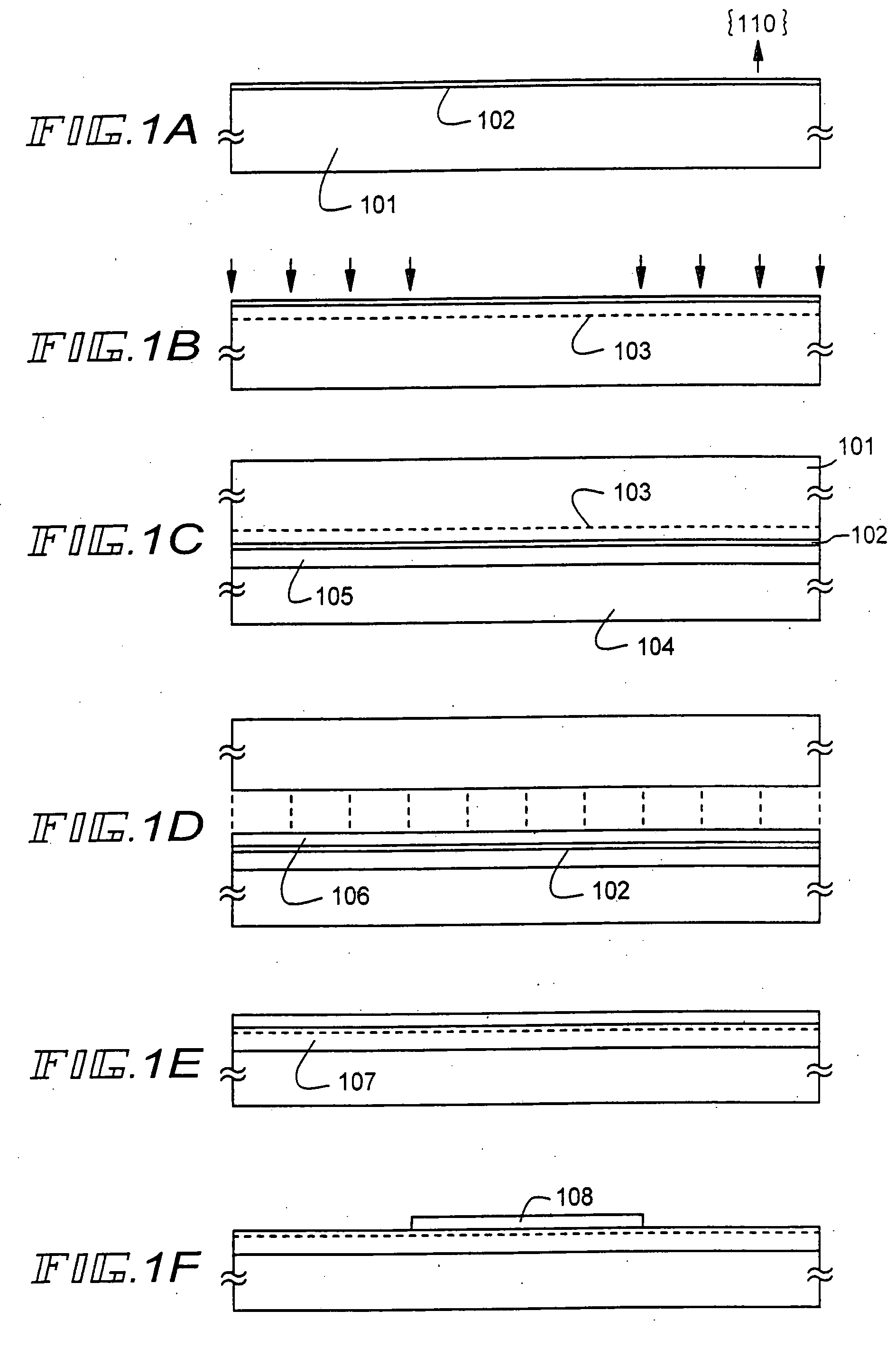
[0057] In this embodiment, with reference to FIGS. 1A to 1F and 2A to 2E, a description will be made on a case where when an SOI substrate is fabricated by a Smart-Cut method. a single crystal silicon substrate having a main surface of a {110} plane is used, and a semiconductor device is fabricated by using the SOI substrate.

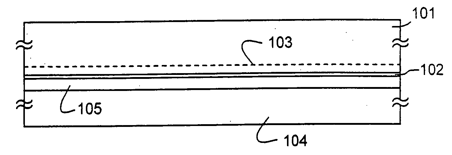
[0058] First, a single crystal silicon substrate 101 as a forming material of a single crystal silicon layer is prepared. Here, although a P-type substrate having a main surface of a crystal face of a {110} plane is used, an N-type substrate may be used. Of course, a single crystal silicon germanium substrate may be used.

[0059] Next, a thermal oxidation treatment is carried out, so that a silicon oxide film 102 is formed on the main surface (corresponding to an element forming surface). Although a film thickness may be suitably determined by a user, the thickness is made 10 to 500 nm (typically 20 to 50 nm). This silicon oxide film 102 functions later as a par...

embodiment 2

[0093] In this embodiment, a description will be made of an example in which an SOI substrate different from that of embodiment 1 is fabricated by using a single crystal silicon substrate having a main surface of a {110} plane, and a semiconductor device is fabricated by using the SOI substrate using FIGS. 3A to 3F. Specifically, a case where a technique called ELTRAN is used will be described.

[0094] First, a single crystal silicon substrate 301 having a main surface (crystal face) of a {110} plane is prepared. Next, the main surface is subjected to anodization to form a porous silicon layer 302. The anodization step may be carried out in a mixed solution of hydrofluoric acid and ethanol. The porous silicon layer 302 is regarded as a single crystal silicon layer provided with columnar surface holes at a surface density of about 1011 holes / cm3, and succeeds to the crystal state (orientation, etc.) of the single crystal silicon substrate 301 as it is. Incidentally, since the ELTRAN m...

embodiment 3

[0111] In this embodiment, a description will be made on an example in which a single crystal silicon substrate having a main surface of a {110} plane is used to fabricate an SOI substrate different from that of embodiment 1 or embodiment 2, and a semiconductor device is fabricated by using the substrate using FIGS. 4A to 4C. Specifically, a case in which an SOI substrate called SIMOX is fabricated will be described.

[0112] In FIG. 4A, reference numeral 401 designates a single crystal silicon substrate. In this embodiment, an oxygen ion is first added to the single crystal silicon substrate 401 to form an oxygen-containing layer 402 at a predetermined depth. The oxygen ion with a dosage of about 1×10¹⁸ atoms / cm2 may be added.

[0113] At this time, since the {110} plane has small atomic density, a probability of collision of the oxygen ion and silicon atom becomes lower. That is, it is possible to suppress damage of the silicon surface due to the addition of oxygen to the minimum. Of ...


PUM


Abstract

A semiconductor device with high reliability is provided using an SOI substrate. When the SOI substrate is fabricated by using a technique typified by SIMOX, ELTRAN, or Smart-Cut, a single crystal semiconductor substrate having a main surface (crystal face) of a {110} plane is used. In such an SOI substrate, adhesion between a buried insulating layer as an under layer and a single crystal silicon layer is high, and it becomes possible to realize a semiconductor device with high reliability.

Description

BACKGROUND OF THE INVENTION [0001] 1. Field of Invention [0002] The present invention relates to a semiconductor device fabricated by using an SOI (Silicon on Insulator) substrate and a method of fabricating the same. Specifically, the invention relates to a semiconductor device including a thin film transistor (hereinafter referred to as TFT) formed on an SOI substrate. [0003] Incidentally, in the present specification, the semiconductor device indicates any device capable of functioning by using semiconductor characteristics. Thus, the semiconductor device includes not only a TFT but also an electro-optical device typified by a liquid crystal display device or a photoelectric conversion device, a semiconductor circuit in which TFTs are integrated, and an electronic equipment containing such an electro-optical device or a semiconductor circuit as a part. [0004] 2. Description of the Related Art [0005] In recent years, VLSI techniques have been remarkably developed, and attention ha...

Claims


Application Information

Patent Timeline
Patent Type & Authority Applications(United States)
IPC IPC(8): H01L21/30H01L27/12H01L21/02H01L21/336H01L21/762H01L29/786
CPCH01L21/76243H01L21/76254H01L21/76256H01L27/1203H01L27/1214Y10S438/973H01L29/045H01L29/66772H01L29/78603Y10S438/977H01L27/1266
Inventor YAMAZAKI, SHUNPEIOHTANI, HISASHI
Owner SEMICON ENERGY LAB CO LTD
Why Eureka
Try Eureka