Actuator chip for inkjet printhead with electrostatic discharge protection

a technology of electrostatic discharge protection and actuator chip, which is applied in the direction of printing, electrical apparatus, basic electric elements, etc., can solve the problems of inoperable, inability to provide adequate esd protection for thinner passivation, and inability to opera

Inactive Publication Date: 2007-08-16
FUNAI ELECTRIC CO LTD
View PDF30 Cites 10 Cited by
  • Summary
  • Abstract
  • Description
  • Claims
  • Application Information

AI Technical Summary

Benefits of technology

[0011] In one embodiment of the invention, an actuator chip includes pluralities of thin film layers on a substrate forming pluralities of actuators. For example, a resistor layer can reside on the substrate with a dielectric layer on the resistor layer, and a cavitation layer on the dielectric layer. (Naturally, intervening layers are possible). ESD protection can be provided by an ESD circuit, one per each actuator, such as a circuit including a ballast resistor in series with a diode. A conductive metal buss can be connected to each ballast resistor on one side and to pluralities of fingers of the cavitation layer, extending from a large mass of the cavitation layer, on another side. In an exemplary embodiment, forward biasing of the diode toward power or away from ground occurs for alternating ones of the ESD circuits and, during ...

Problems solved by technology

However, as layers continued to become thinner and more energy efficient over time, thinner passivation seemed unable to provide adequate ESD protection.
It some instances, the passivation has been so thin that ESD events damage the resistor layer making it altogether inoperable.
However, a disparity exists between heaters closest to the serpentine structure and those farther away.
However, these approaches add undesirable complexity.
For example, using devices that are not practically reset able, like conventional fuses and/or preferred breakdown locations, can obviously limit the functionality of such circ...

Method used


Image

  • Actuator chip for inkjet printhead with electrostatic discharge protection
  • Actuator chip for inkjet printhead with electrostatic discharge protection
  • Actuator chip for inkjet printhead with electrostatic discharge protection

Examples


Embodiment Construction

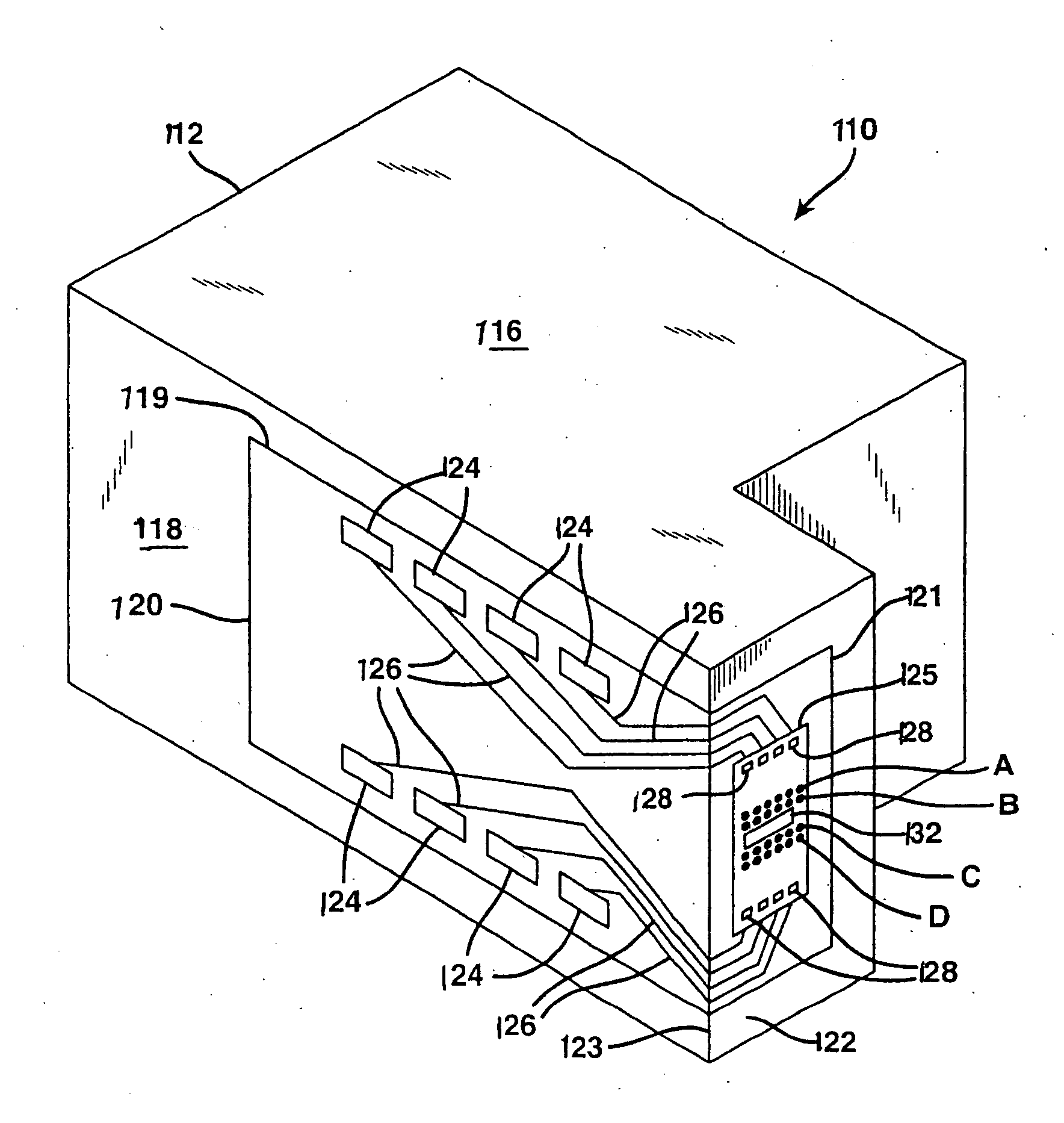
[0023] In the following detailed description of exemplary embodiments, reference is made to the accompanying drawings that form a part hereof, and in which is shown by way of illustration, specific embodiments in which the invention may be practiced. These embodiments are described in sufficient detail to enable those skilled in the art to practice the invention, and it is to be understood that other embodiments may be utilized and that process, electrical or mechanical changes may be made without departing from the scope of the present invention. The term wafer or substrate used in this specification includes, for example, ceramic and silicon substrates. For example, embodiments of the present invention might use silicon-on-sapphire (SOS) technology, silicon-on-insulator (SOI) technology, thin film transistor (TFT) technology, doped and undoped semiconductors, epitaxial layers of silicon supported by a base semiconductor structure, as well as other structures well known to one skil...


PUM


Abstract

An inkjet printhead chip includes electrostatic discharge (ESD) circuits to protect the chip during ESD events, such as one especially to prevent a thin dielectric layer on a substrate from breakdown. In one embodiment, the chip includes an ESD circuit essentially dedicated per each actuator. In another, ESD circuits alternate connection between power and ground. In still another, actuators are approximately equidistantly spaced with respect to respective ESD circuits. Exemplary ESD circuits include a ballast resistor in series with a diode. In turn, diodes are either forward biased toward power or away from ground. In a thermal inkjet embodiment, a cavitation layer above a resistor and dielectric layer have pluralities of fingers connecting the cavitation layer to a metal buss. The metal buss attaches to the ballast resistors. Protection typically embodies the safe distribution of ESD current to ground during both chip manufacture and user printhead installation. Inkjet printheads and printers are also disclosed.

Description

FIELD OF THE INVENTION [0001] The present invention relates to inkjet printheads. In particular, it relates to an actuator chip having electrostatic discharge (ESD) protection. BACKGROUND OF THE INVENTION [0002] The art of printing images with inkjet technology is relatively well known. In general, an image is produced by emitting ink drops from a printhead at precise moments so they impact a print medium at a desired location. In a scanning-head embodiment, the printhead is supported by a movable print carriage within a device, such as an inkjet printer, and is caused to reciprocate relative to an advancing print medium. It emits ink at times pursuant to commands of a microprocessor or other controller. The timing of the emissions corresponds to a pattern of pixels of the image being printed. Other than printers, familiar devices incorporating inkjet technology include fax machines, all-in-ones, photo printers, and graphics plotters, to name a few. [0003] Conventionally, a thermal ...

Claims


Application Information

Patent Timeline
IPC IPC(8): B41J2/015
CPCB41J2/04511B41J2/14072B41J2/0458B41J2/04541
Inventor YOUNG, JASON K.RODRIGUEZ, NICOLE M.
Owner FUNAI ELECTRIC CO LTD
Why Eureka
Try Eureka