

Photolithographic patterning of polymeric materials
a polymer material and photolithographic technology, applied in the direction of synthetic resin layered products, nuclear engineering, railway components, etc., can solve the problems of compromising the operation of the device, affecting the lithographic patterning effect, and unable to etch fine features
- Summary
- Abstract
- Description
- Claims
- Application Information
AI Technical Summary
Benefits of technology
Problems solved by technology
Method used
Image

Examples
example 1
CONVENTIONAL METHOD OF COATING ON SILICON SUBSTRATE
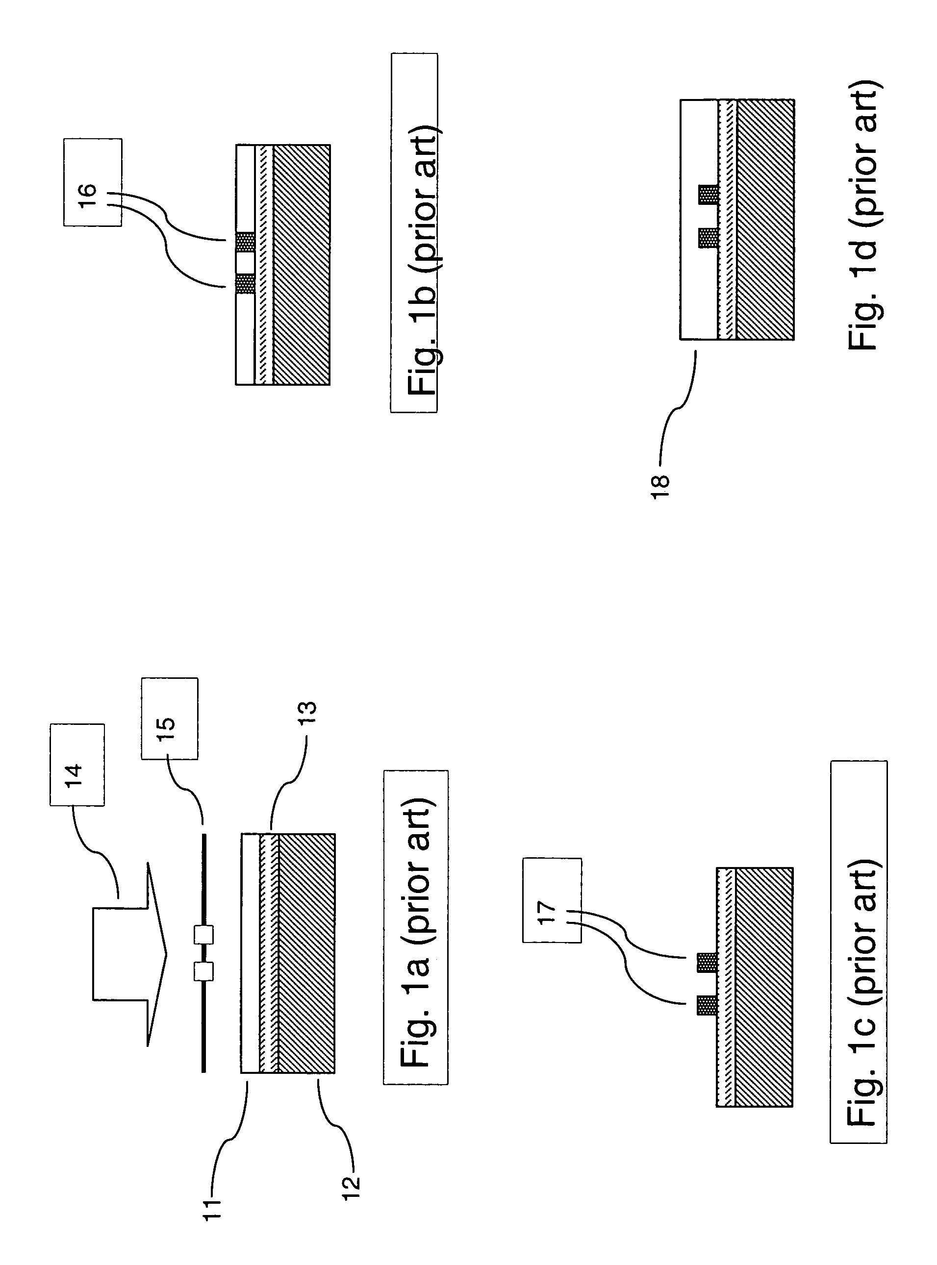
[0069] Following the procedure disclosed in U.S. Pat. No. 6,818,721, a lower refractive index polymer A was prepared with a viscosity of 2500 cP (at 20° C.) and a refractive index (measured at 20° C. on an Abbé refractometer with room light) of 1.483. A higher refractive index polymer B was prepared with a viscosity of 2200 cP (at 20° C.) and a refractive index of 1.509 (at 20° C.). The free radical generating photo-initiator Irgacure 369 was added to both polymer A and polymer B at a level of 2 wt %. Methacrylate-containing substituents were borne by 25% of the silicon atoms in polymers A and B.
[0070] Polymer A was spin coated onto a silicon wafer and cured with UV light from a mercury lamp in an Oriel flood illuminator to form a lower cladding layer 20 μm thick and with a refractive index of 1.478 (at 20° C. and 1550 nm). Polymer B was spin coated onto the lower cladding to form a core layer 11 μm thick, and imagewise exposed to ...
example 2
CONVENTIONAL METHOD OF COATING ON POLYCARBONATE SUBSTRATE
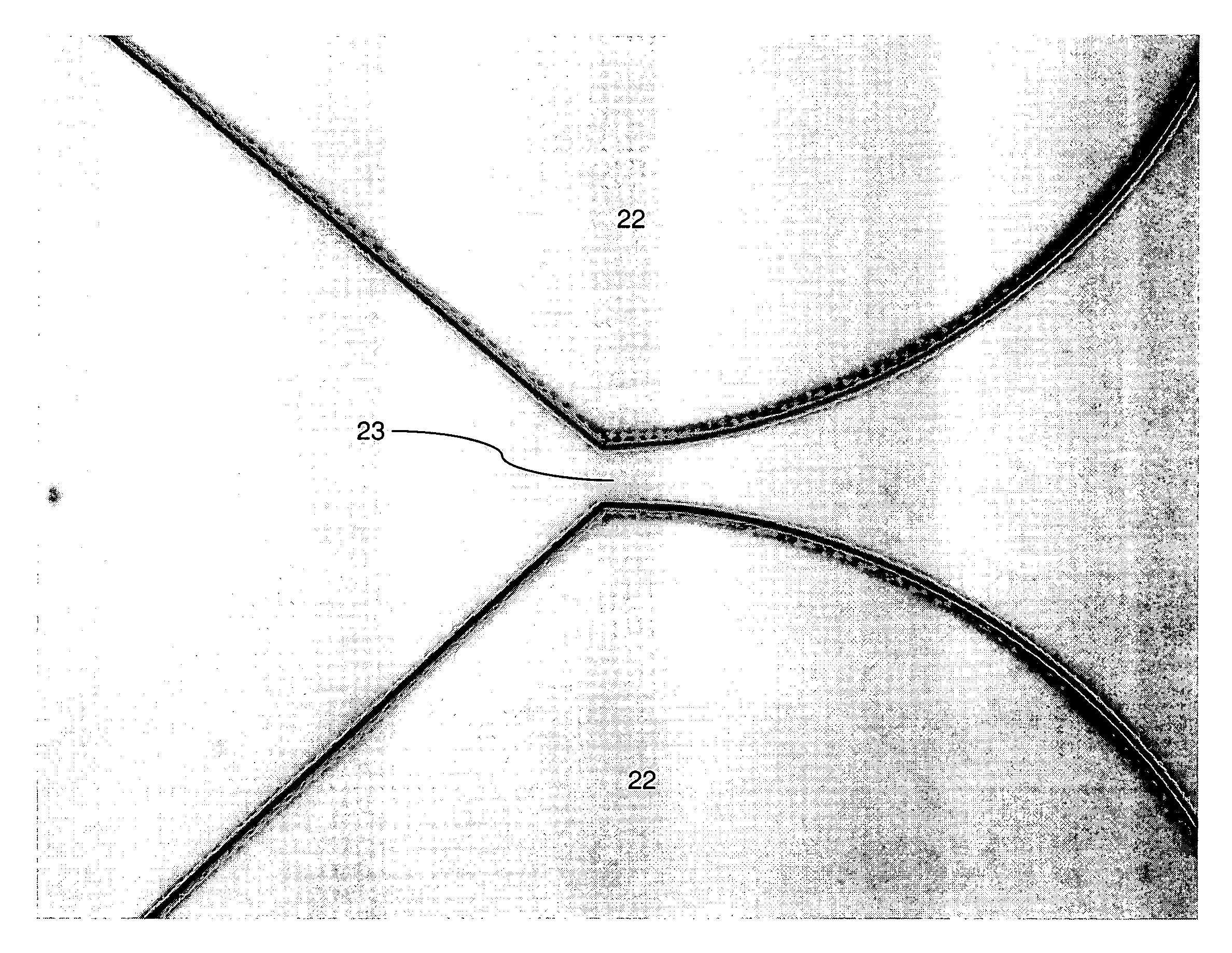
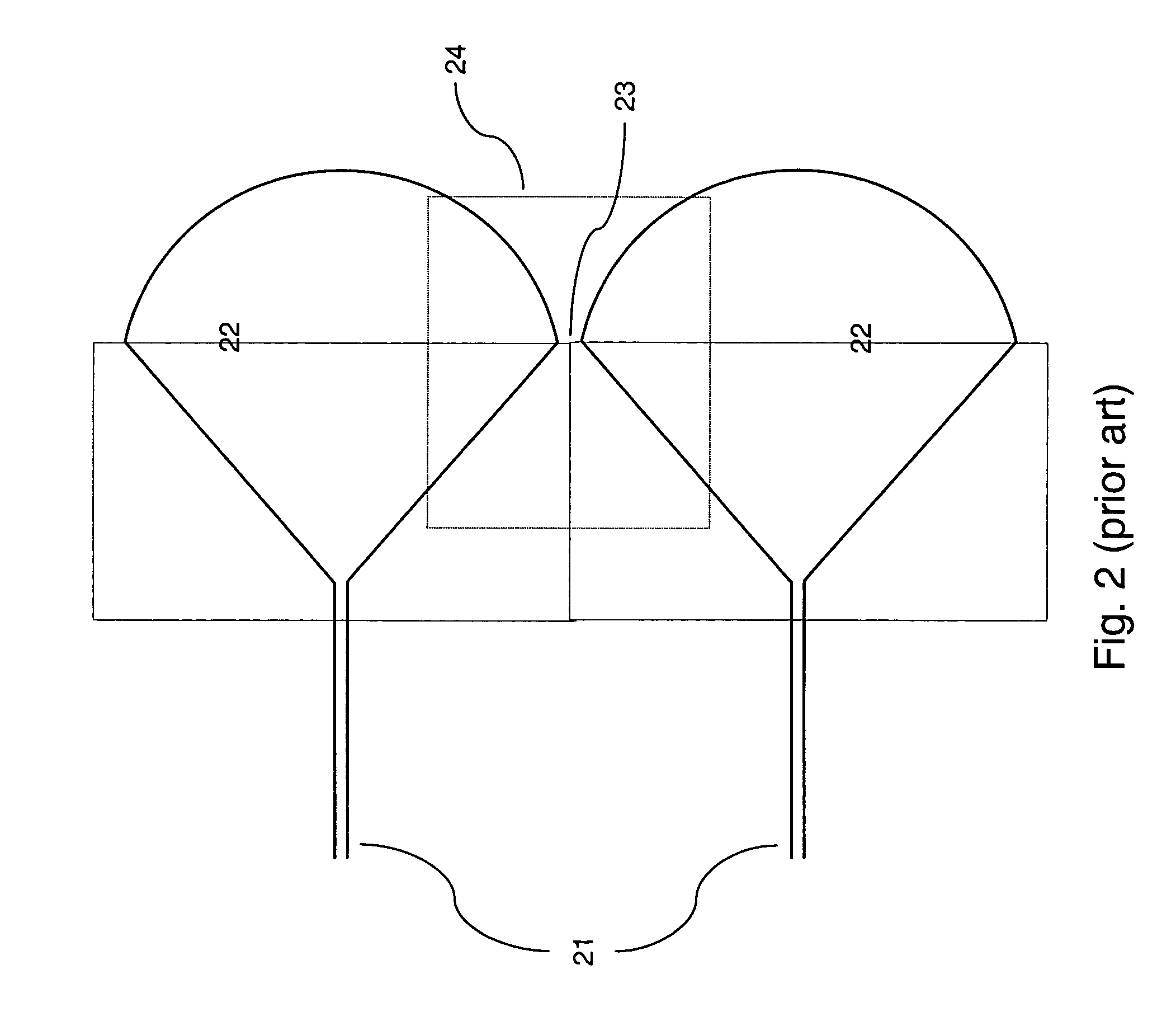
[0071] The processing conditions in this example are identical to those in Example 1 except that the substrate was polycarbonate (DE1-1, Bayer) instead of silicon. In this case a photograph (FIG. 4) shows roughness 41 on the sidewalls of lenses 22 and a considerable amount of polymerised material 42 in gap 23 between the lenses.
example 3
CONVENTIONAL METHOD OF COATING ON PET SUBSTRATE
[0072] The processing conditions in this example are identical to those in Example 1 except that the substrate was PET (Melinex® 518, Dupont) instead of silicon. Similar to the case of Example 2, a photograph (FIG. 5) shows roughness 41 on the sidewalls of lenses 22 and a considerable amount of polymerised material 42 in gap 23 between the lenses.
[0073] The effect caused by the change of substrate from silicon to PET or polycarbonate was surprising and striking. In some manner, changing from a silicon substrate to a plastic substrate has altered the polymerisation dynamics of the curable composition. The ability to photo-imprint features with high contrast depends, among other factors, on the balance between the rate of free radical generation and the rate of free radical scavenging by oxygen dissolved or present in the photo-curable material. Without wishing to be bound by theory, it is believed that the presence of the plastic has so...
PUM
| Property | Measurement | Unit |
|---|---|---|
| refractive index | aaaaa | aaaaa |
| Tg | aaaaa | aaaaa |
| width | aaaaa | aaaaa |
Abstract
Description
Claims
Application Information