Poly pre-doping anneals for improved gate profiles

a technology of polysilicon gates and gate profiles, applied in the direction of semiconductor/solid-state device manufacturing, basic electric elements, electric apparatus, etc., can solve the problems of irregular gate profiles, deviating substantially from the ideal vertical sidewall, and difficult to control the vertical profile of polysilicon gates

Inactive Publication Date: 2007-08-23
FREESCALE SEMICON INC
View PDF5 Cites 38 Cited by
  • Summary
  • Abstract
  • Description
  • Claims
  • Application Information

AI Technical Summary

Problems solved by technology

Each type of processing may contribute separately to the etching of the polysilicon gate, making it difficult to control the vertical profiles of polysilicon gates.
These etch and clean steps—in conjunction with doping, nitrogen implant (for PMOS gates) and implant damage—result in an irregular gate profile that, in many cases, deviates substantially from the ideal vertical sidewall.
Such irregular or non-vertical sidewalls can adversely affect gate dimension control, short channel effect (SCE) control, and silicidation robustness, thereby negatively impacting circuit performance and yield.

Method used


Image

  • Poly pre-doping anneals for improved gate profiles
  • Poly pre-doping anneals for improved gate profiles
  • Poly pre-doping anneals for improved gate profiles

Examples


Embodiment Construction

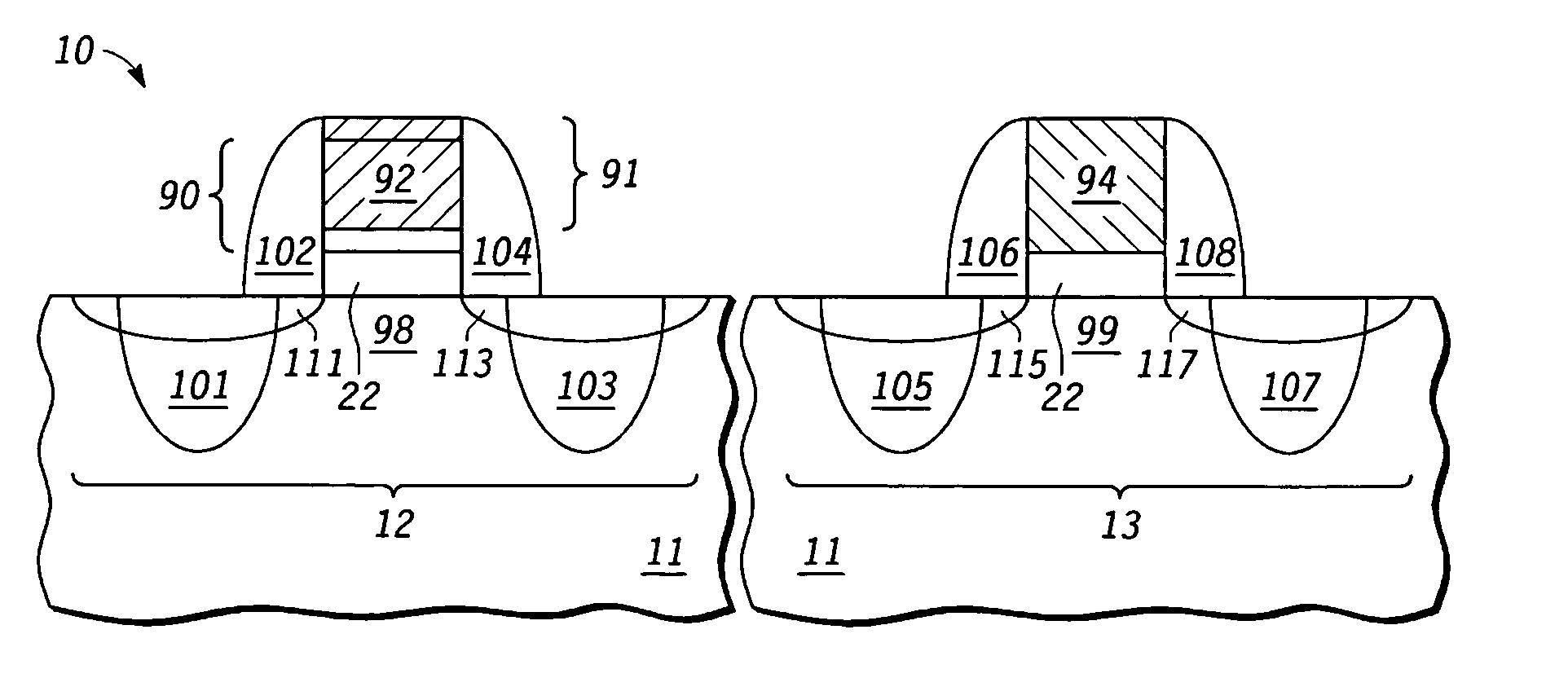
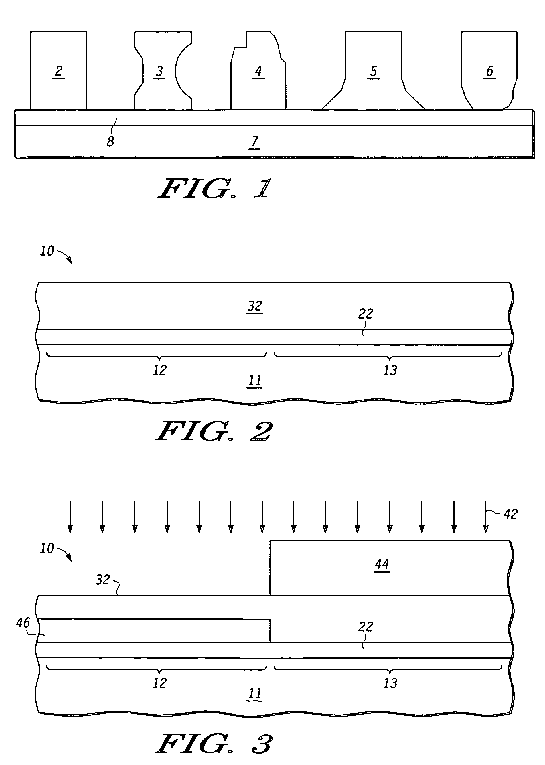
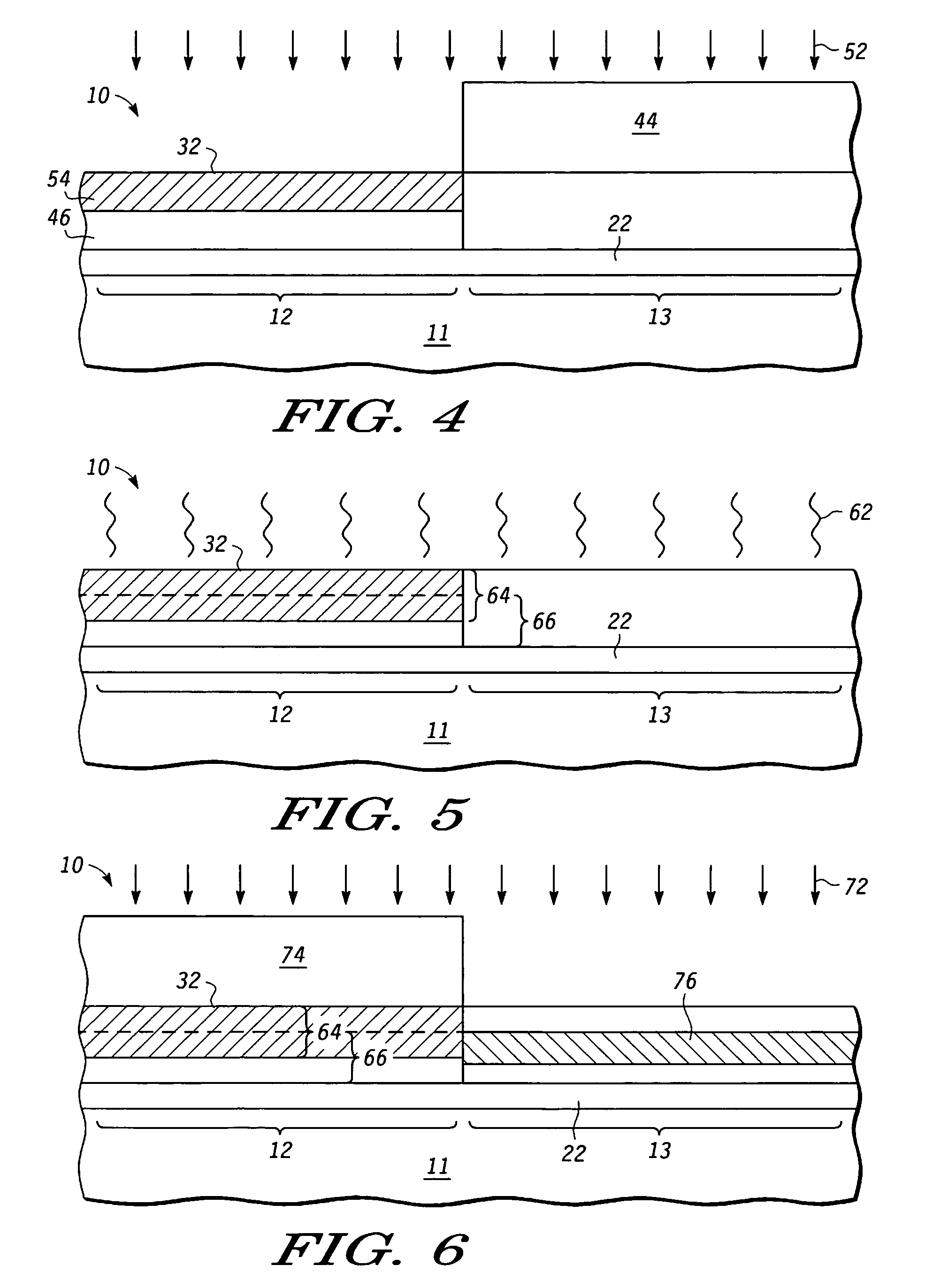
[0017] A method and apparatus are described for fabricating a silicon-based device feature, such as a gate, by implanting a layer of undoped gate electrode material (such as polysilicon, single crystalline silicon, amorphous silicon, silicon germanium or the like) with an implant species (e.g., nitrogen), and then applying one or more rapid thermal anneal processes, either before or after subsequent pre-doping of the polysilicon layer. By annealing the implanted nitrogen and pre-doping implants before gate etching is performed, the subsequently etched gates have improved, more vertical profiles. The profile control provided by various embodiments of the present invention improves yield by improving critical dimension control at the bottom of the gates, provides robust silicide formation at the top of the gates, and extends existing silicide technologies to smaller dimensions. For example, when existing cobalt silicide layers are formed on polysilicon gate electrodes, the increased s...


PUM


Abstract

A semiconductor process and apparatus uses a predetermined sequence of patterning and etching steps to etch a gate stack (32) formed over a substrate (11), thereby forming an etched gate (92, 94) having a vertical sidewall profile by implanting the gate stack (32) with a nitrogen (42) and a dopant (52) and then heating the polysilicon gate stack (32) at a selected temperature using rapid thermal annealing (62) to anneal the nitrogen and dopant so that subsequent etching of the polysilicon gate stack (32) creates an etched gate (92, 94) having more idealized vertical gate sidewall profiles.

Description

BACKGROUND OF THE INVENTION [0001] 1. Field of the Invention [0002] The present invention is directed in general to the field of semiconductor devices. In one aspect, the present invention relates to controlling the profile of semiconductor features in semiconductor devices. [0003] 2. Description of the Related Art [0004] As semiconductor device sizes are scaled down, the requirements for device design and fabrication continue to be tightened in order to fit more circuitry on smaller chips. As device sizes shrink, increasingly complex etch processes are used to define semiconductor device features, such as polysilicon gates. For example, a typical gate patterning process may use several steps after the doped polysilicon layer is formed and the photoresist (“PR”) is patterned, including a PR trim step (to shrink the size of the features being transferred), a hard mask etch step (which uses the PR as a mask), an ARC etch step (which uses the hard mask as a mask), a preliminary cleanin...

Claims


Application Information

Patent Timeline
Patent Type & Authority Applications(United States)
IPC IPC(8): H01L21/336
CPCH01L21/28035H01L21/28123H01L21/823828H01L21/823437H01L21/32155
Inventor SHROFF, MEHUL D.HALL, MARK D.GRUDOWSKI, PAULSTEPHENS, TAB A.STOUT, PHILLIP J.ADETUTU, OLUBUNMI O.
Owner FREESCALE SEMICON INC
Why Eureka
Try Eureka