Entire encapsulation of Cu interconnects using self-aligned CuSiN film

Inactive Publication Date: 2007-08-23
ALSEPHINA INNOVATIONS INC
View PDF12 Cites 31 Cited by
  • Summary
  • Abstract
  • Description
  • Claims
  • Application Information

AI Technical Summary

Benefits of technology

[0027] Similarly, some advantages are applicable to one aspect of the invention, and inapplicable to others. Furthermore, certain aspects of the claimed invention have not been discussed herein. However, no inference should be drawn regarding those discussed herein relative to those not discussed herein oth

Problems solved by technology

While several processing difficulties related to forming copper semiconductor features have been overcome, several problems remain, especially in the areas of current leakage between copper interconnects and the increased tendency of copper to electro-migrate through low-k porous dielectric insulating layers.
One problem affecting copper metallization is the tendency of copper to easily form oxides of copper, for example CuO or CuO2, upon exposure to oxidizing environments including humid environments.
The dual goals of preventin

Method used


Image

  • Entire encapsulation of Cu interconnects using self-aligned CuSiN film
  • Entire encapsulation of Cu interconnects using self-aligned CuSiN film

Examples


Embodiment Construction

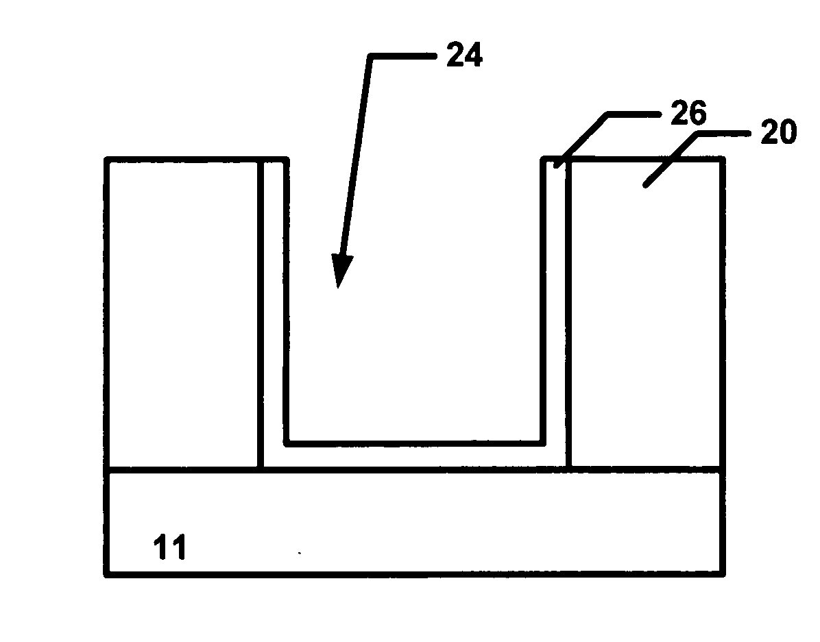
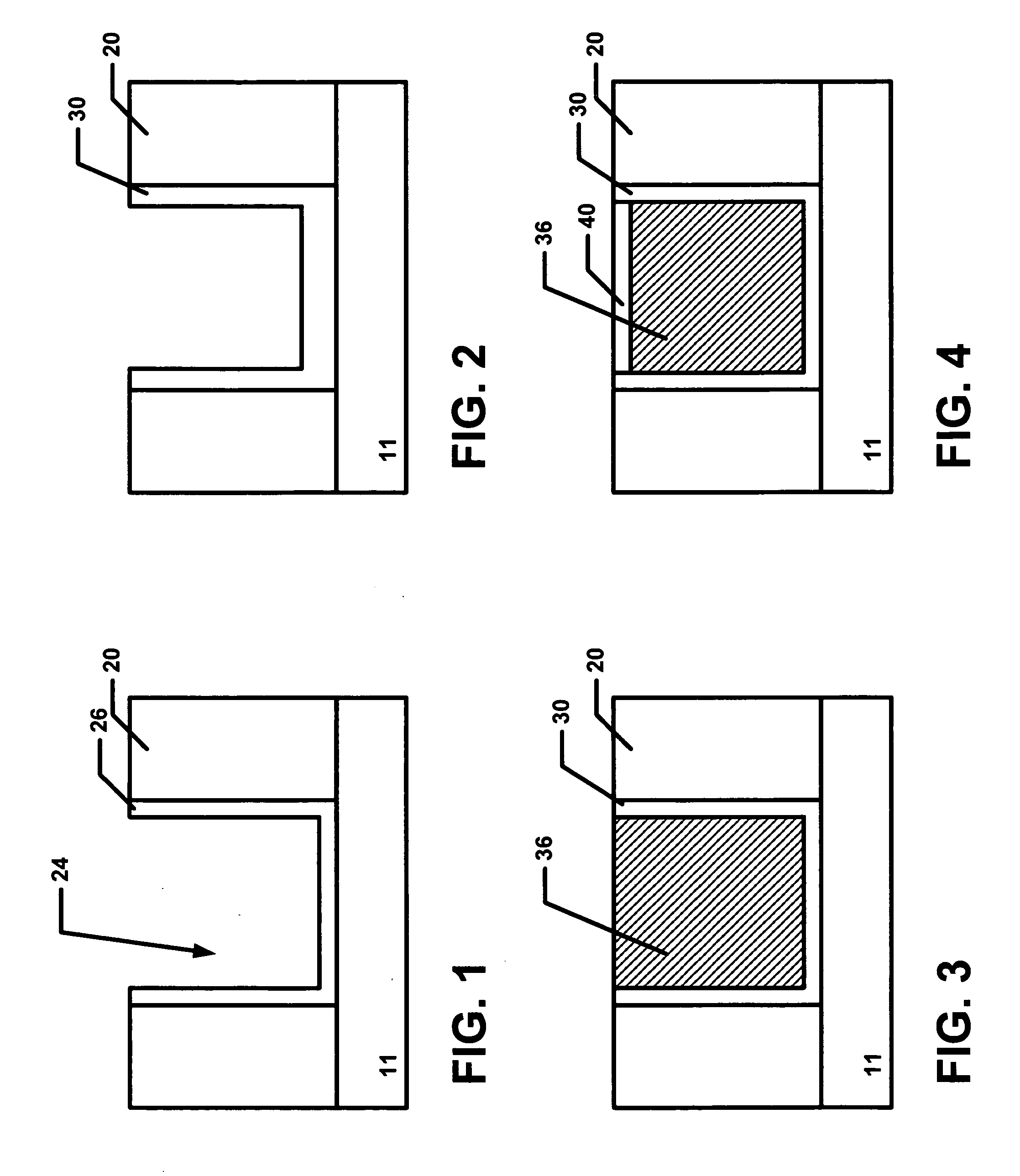
[0030] In an exemplary embodiment, referring to FIGS. 1-4, are shown cross sectional views of a portion of a multi-level semiconductor device at stages in an interconnect manufacturing process.

[0031] A. Provide an Interconnect Opening in a Dielectric Layer over a Semiconductor Structure

[0032] Referring to FIG. 1, we provide an interconnect opening 24 in a dielectric layer 20 over a semiconductor structure 11.

[0033] The semiconductor structure 11 can comprise a substrate with devices (e.g., FETs) formed within and thereon. The substrate can be a semiconductor substrate, such as a silicon wafer or a SOI substrate. The dielectric layer 20 can be a interlevel dielectric (ILD) layer or inter metal dielectric (IMD ) layer. The dielectric layer 20 can have a thickness between 3000 and 6000 angstroms. The dielectric layer can be comprised of a low K dielectric such as SiCOH.

[0034] The interconnect opening 24 can expose a conductive structure, such as a lower level interconnect or contac...


PUM


Abstract

A method of forming a barrier layer and cap comprised of CuSiN for an interconnect. We provide an interconnect opening in a dielectric layer over a semiconductor structure. We form a CuSiN barrier layer over the sidewalls and bottom of the interconnect opening by reacting with the first copper layer. We then form an interconnect over the CuSiN layer filling the interconnect opening. We can form a CuSiN cap layer on the top surface of the interconnect.

Description

BACKGROUND OF INVENTION [0001] 1) Field of the Invention [0002] This invention relates generally to fabrication of semiconductor devices and more particularly to the formation of barrier layer for interconnects and more particularly for formation of a copper and silicon and nitrogen containing barrier layer. [0003] 2) Description of the Prior Art [0004] Copper metallization is increasingly being used for advanced semiconductor device integrated circuit fabrication including semiconductor features having sub-quarter micron linewidths and high aspect ratios to larger features such as bonding pads. Copper and its alloys have lower resistivity and better electromigration resistance compared to other metals such as, for example, aluminum. These characteristics are critical for achieving device reliability together with higher current densities and increased signal propagation speed. While several processing difficulties related to forming copper semiconductor features have been overcome,...

Claims


Application Information

Patent Timeline
IPC IPC(8): H01L21/4763
CPCH01L21/76843H01L2924/01047H01L21/76856H01L24/03H01L24/05H01L2224/05073H01L2224/05546H01L2224/05647H01L2924/01013H01L2924/01014H01L2924/01022H01L2924/01029H01L2924/01073H01L2924/01074H01L2924/01078H01L21/76849H01L2924/01033H01L2924/01023H01L2924/01019H01L2924/01005H01L2924/01006H01L2924/01039H01L2924/14H01L2924/00
Inventor WIDODO, JOHNNYZHANG, BEI CHAOCHEN, TONG QINGSIEW, YONG KONGZHANG, FANLIEW, SAN LEONGSUDIJONO, JOHNHSIA, LIANG CHOO
Owner ALSEPHINA INNOVATIONS INC
Why Eureka
Try Eureka