Two-Level RAM Lookup Table for Block and Page Allocation and Wear-Leveling in Limited-Write Flash-Memories
Inactive Publication Date: 2007-08-30
SUPER TALENT TECH CORP
View PDF17 Cites 259 Cited by
Summary
Abstract
Description
Claims
Application Information
AI Technical Summary
This helps you quickly interpret patents by identifying the three key elements:
Problems solved by technology
Method used
Benefits of technology
Problems solved by technology
However, since flash memory chips are block-addressable rather than randomly-accessible, flash is not as easy to use for a cache as DRAM or SRAM.
However, MLC flash chips may impose additional restrictions on usage.
For example, a MLC flash chip may not allow pages to be written a second time before erase, such as for number-of-page-programming NOP=1 chips.
Some MLC flash chips may be even more restrictive.
These restrictive MLC chips may prohibit “backwards” writing, but only allow “forw
Method used
Image
Click on the blue label to locate the original text in one second.
Reading with bidirectional positioning of images and text.
Examples
Embodiment Construction
[0025] The present invention relates to an improvement in flash memory controllers. The following description is presented to enable one of ordinary skill in the art to make and use the invention as provided in the context of a particular application and its requirements. Various modifications to the preferred embodiment will be apparent to those with skill in the art, and the general principles defined herein may be applied to other embodiments. Therefore, the present invention is not intended to be limited to the particular embodiments shown and described, but is to be accorded the widest scope consistent with the principles and novel features herein disclosed.
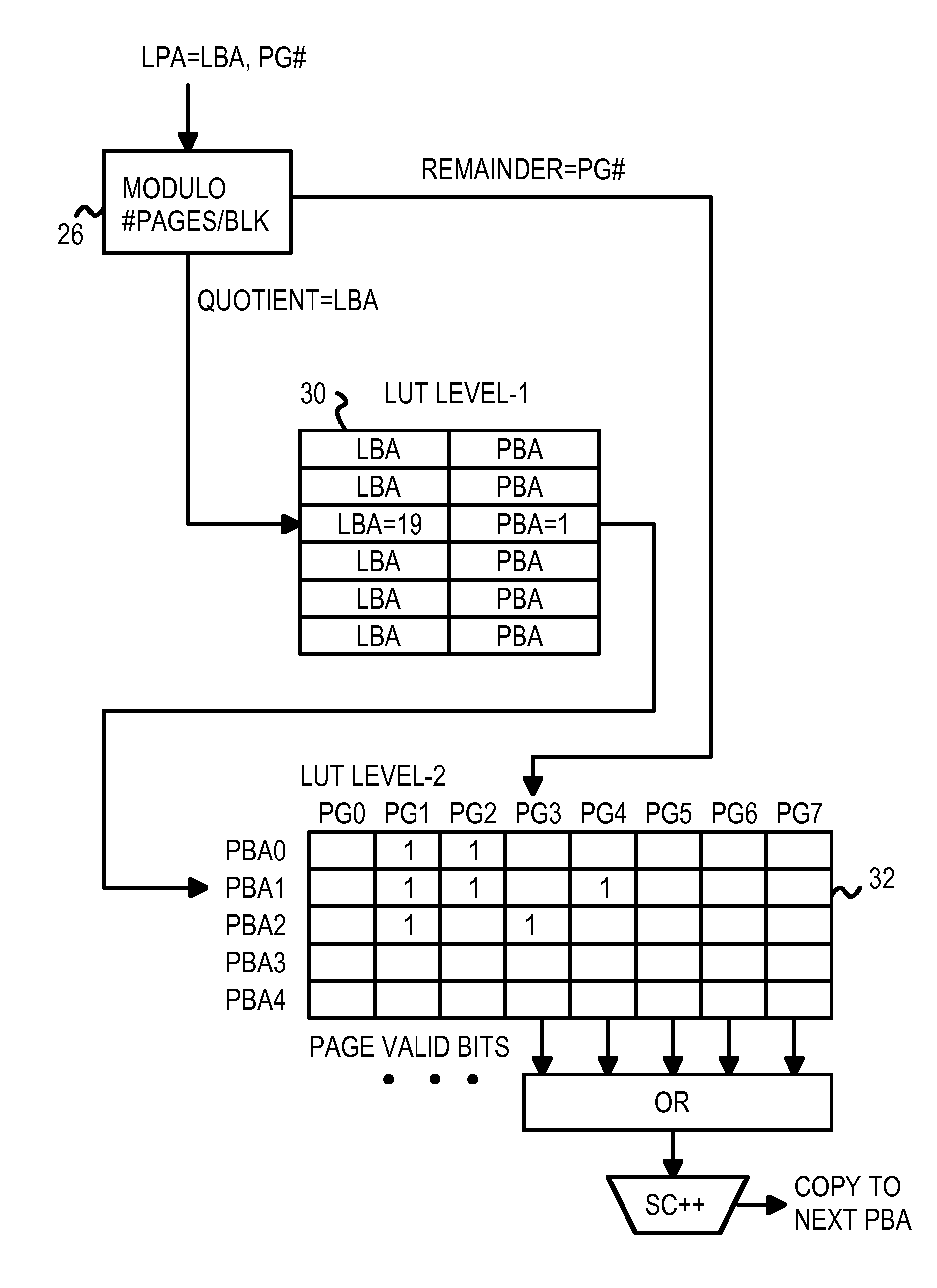
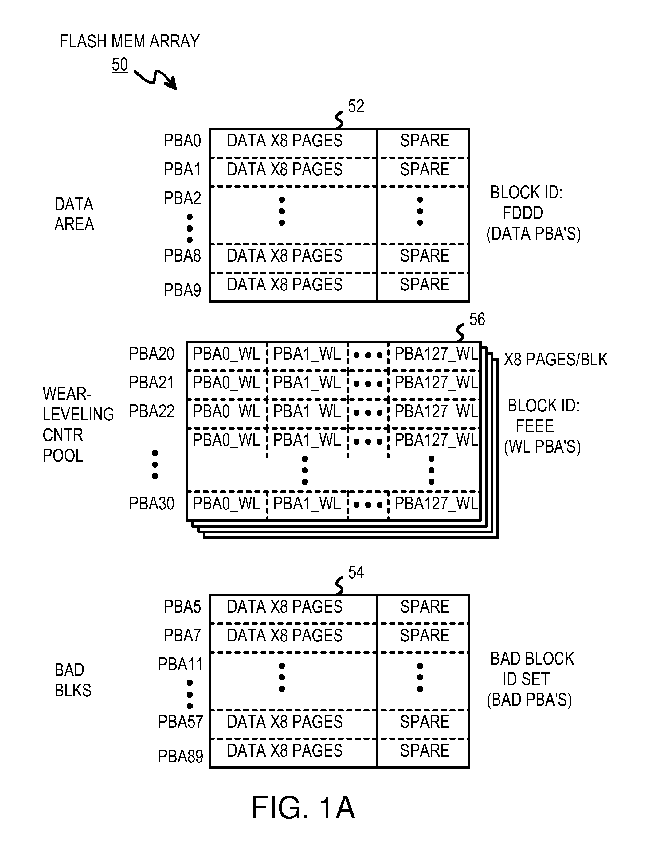
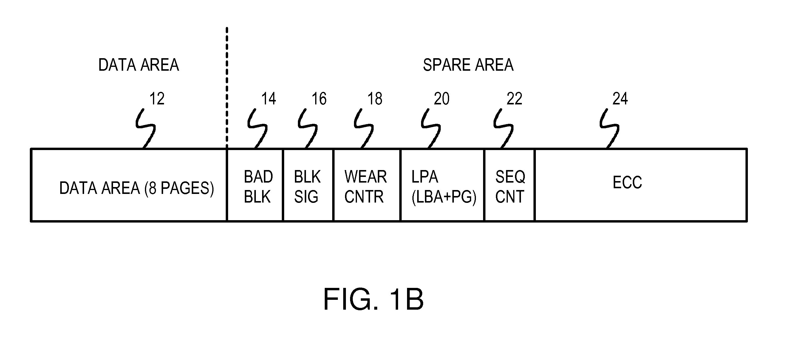
[0026]FIG. 1A shows an arrangement of physical blocks in a flash-memory array. Flash-memory array 50 contains one or more MLC flash-memory chips that are block-addressable. The data in a block may be erased to all 1's, and then written with 0's. However, data may not be written from 0 back to 1 without erasing the whole blo...
PUM
Abstract
A restrictive multi-level-cell (MLC) flash memory prohibits regressive page-writes. When a regressive page-write is requested, an empty block having a low wear-level count is found, and data from the regressive page-write and data from pages stored in the old block are written to the empty block in page order. The old block is erased and recycled. A two-level look-up table is stored in volatile random-access memory (RAM). A logical page address from a host is divided by a modulo divider to generate a quotient and a remainder. The quotient is a logical block address that indexes a first-level look-up table to find a mapping entry with a physical block address that selects a row in a second-level look-up table. The remainder locates a column in the row in the second-level look-up table. If any page-valid bits above the column pointed to by the remainder are set, the write is regressive.
Description
RELATED APPLICATION [0001] This application is a continuation-in-part of the co-pending application for “Flash Card Systems”, U.S. Ser. No. 10 / 957,089, filed Oct. 1, 2004. [0002] This application is related to “Flash memory device and architecture with multi level cells”, U.S. Ser. No. 10 / 800,228, filed Mar. 12, 2004, now U.S. Pat. No. 7,082,056, and “Flash drive / reader with serial-port controller and flash-memory controller mastering a second RAM-buffer bus parallel to a CPU bus”, U.S. Ser. No. 10 / 605,140, filed Sep. 10, 2003, now U.S. Pat. No. 6,874,044.FIELD OF THE INVENTION [0003] This invention relates to multi-bit-cell (MBC) or multi-level-cell (MLC) flash-memory systems, and more particularly to sequencing of page writes in restricted-write memories. BACKGROUND OF THE INVENTION [0004] Rotating hard-disk drives are often used in personal computers (PC's), servers, video recorders, and many other kind of electronic devices for mass storage. Mass storage is used to store large a...
Claims
Application Information
Patent Timeline
Application Date:The date an application was filed.
Publication Date:The date a patent or application was officially published.
First Publication Date:The earliest publication date of a patent with the same application number.
Issue Date:Publication date of the patent grant document.
PCT Entry Date:The Entry date of PCT National Phase.
Estimated Expiry Date:The statutory expiry date of a patent right according to the Patent Law, and it is the longest term of protection that the patent right can achieve without the termination of the patent right due to other reasons(Term extension factor has been taken into account ).
Invalid Date:Actual expiry date is based on effective date or publication date of legal transaction data of invalid patent.