
Eureka
For R&D, Eureka makes reading and utilizing patents & technical documents easy.
Eureka AIR
Designed for self-driven R&D workflows. Generate viable solutions, solve complex R&D challenges, empower your innovation with AI.

Eureka Materials
Designed for material experts only. Revolutionize your material R&D, from search, analyze, to developing new materials.

TechResearch
Generate reliable direction feasibility study reports for your R&D in just a few steps.

TechSeek
Discover and master advanced knowledge NOW. Basics, ideas, possibilities, all at once.

TechMind
As an expert in R&D Theories, TechMind can generates customized viable solutions instantly.

TechRisk
Analyze your overall solution with one click, know your potential R&D risks in advance.

TechMonitor
Get weekly tech updates, stay abreast of the latest tech innovations and key insights.
Semiconductor device
- Summary
- Abstract
- Description
- Claims
- Application Information
AI Technical Summary
Benefits of technology
Problems solved by technology
Method used
Image

Examples
first embodiment
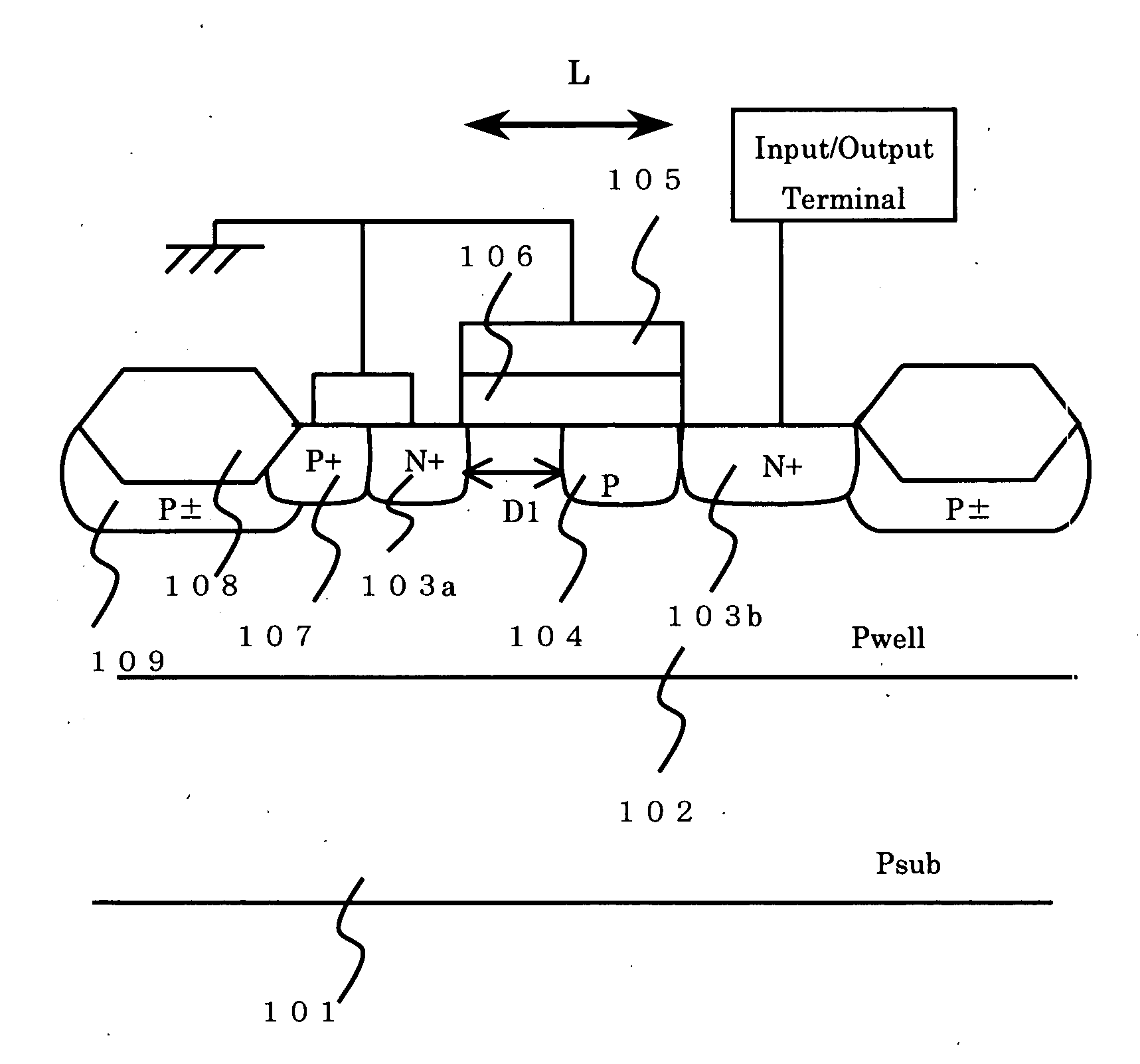
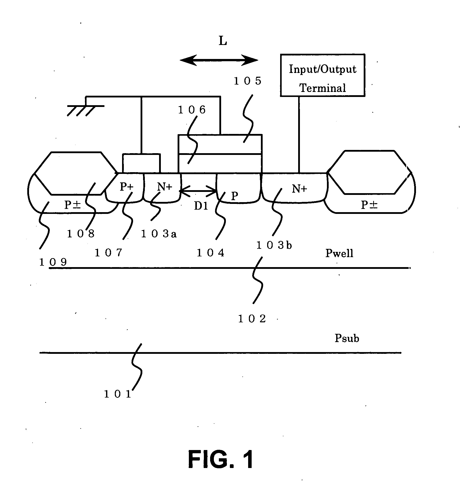
[0015]FIG. 1 is a schematic sectional diagram of an NMOS transistor having a conventional drain structure of a semiconductor device according to a first embodiment of the present invention.
[0016] The NMOS transistor includes a P-type well region 102 formed on a P-type silicon semiconductor substrate 101, a gate oxide film 106 and a polysilicon gate electrode 105 which are formed on the P-type well region 102, a P-type diffusion layer 104 having a high concentration which is formed locally between an N-type source diffusion layer 103a and an N-type drain diffusion layer 103b, which are formed on a surface of a silicon substrate at both ends of the gate electrode and have a high concentration, and a P-type diffusion layer 107 which is provided so as to take a potential of the P-type well region 102, and has a high concentration. N-type drain diffusion layer 103b is connected to an input / output terminal through wiring, and the N-type source diffusion layer 103a, the P-type diffusion l...
second embodiment
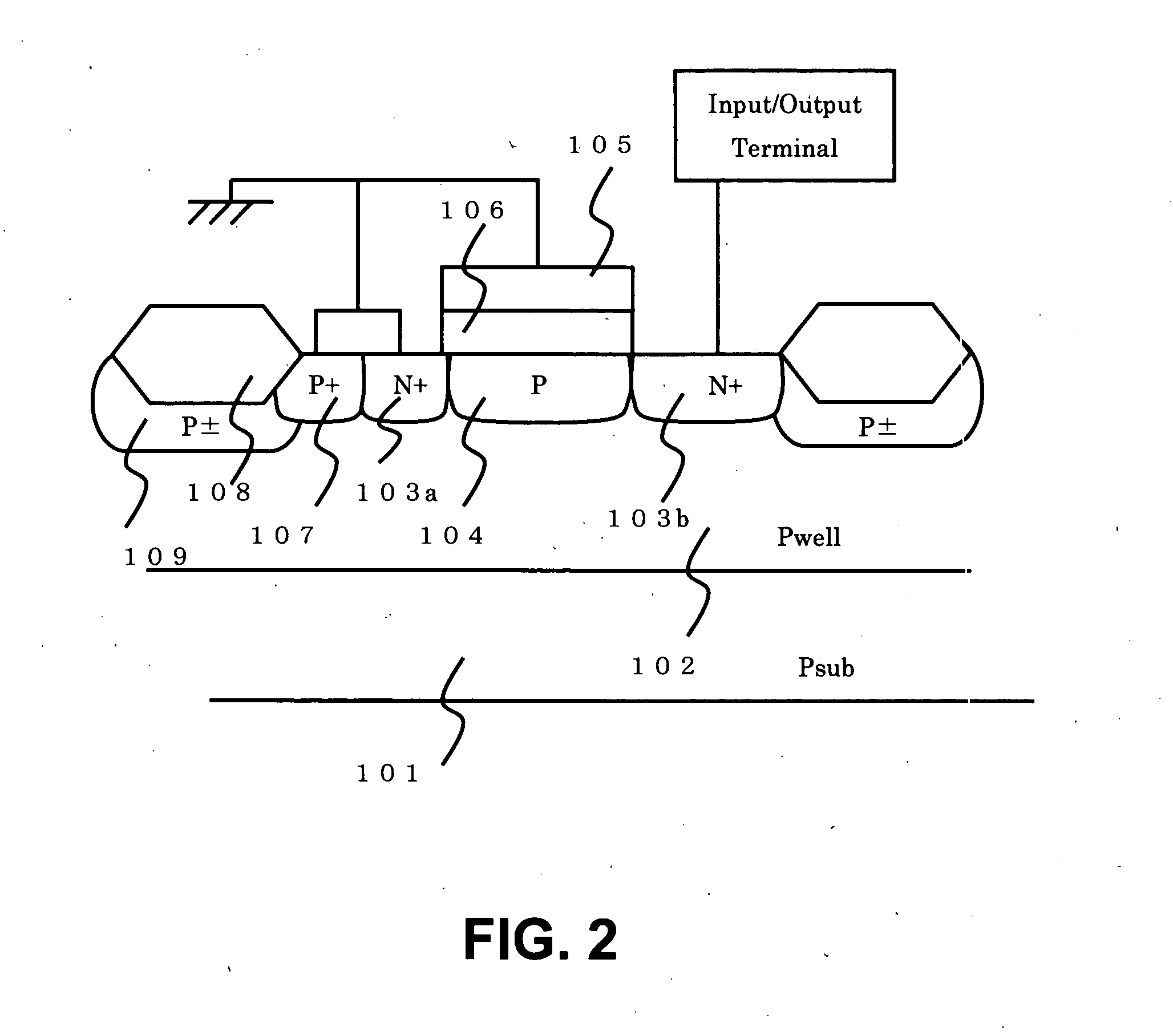
[0021]FIG. 2 is a schematic sectional diagram of an NMOS transistor having a conventional drain structure of a semiconductor device according to a second embodiment of the present invention.
[0022] As shown in FIG. 2, a P-type diffusion layer may be formed on an entire area provided immediately below a gate between N-type source and drain diffusion layers.
PUM
 Abstract
Description
Claims
Application Information
 - R&D Engineer
- R&D Manager
- IP Professional
- Industry Leading Data Capabilities
- Powerful AI technology
- Patent DNA Extraction
Browse by: Latest US Patents, China's latest patents, Technical Efficacy Thesaurus, Application Domain, Technology Topic, Popular Technical Reports.
© 2024 PatSnap. All rights reserved.Legal|Privacy policy|Modern Slavery Act Transparency Statement|Sitemap|About US| Contact US: help@patsnap.com