Scanning electron microscope and a method for imaging a specimen using the same

a scanning electron microscope and specimen technology, applied in the field of scanning electron microscope, can solve the problems of high labor and time required for creating imaging recipes, low automation rate of imaging recipe creation, and inability of sem operators to be indebted to a large reduction of work time, so as to speed up the matching process and achieve high matching accuracy.

Active Publication Date: 2007-09-13
HITACHI HIGH-TECH CORP
View PDF0 Cites 42 Cited by
  • Summary
  • Abstract
  • Description
  • Claims
  • Application Information

AI Technical Summary

Benefits of technology

[0020] (5) For registration of the registry template, the aforementioned CAD data template, modified CAD data template, CAD image template or modified CAD image template is selectively or totally registered in the imaging recipe in accordance with the matching scheme between the actual image template plate and the registry template, so that speedup of the matching process and the high accuracy of matching can be achieved.

Problems solved by technology

In the prior art, problems as below are encountered in creating an imaging recipe used when a plurality of observation points on a specimen are imaged sequentially by using a scanning electron microscope.
As miniaturization of the semiconductor pattern advances, the number of EP's to be inspected increases, raising a problem that much labor and time are necessary for creation of the imaging recipe.
As for automatic selection of AP coordinates, the aforementioned Patent Document gives a description “a characteristic pattern part is automatically detected” but fails to describe a specified method therefore and besides other information to be designated in the imaging recipe and regarding, for example, the necessity / needlessness of setting individual imaging points (AP, AF, AST, ABCC), the number of imaging points, the coordinates and size / shape of each imaging point, the imaging condition and the imaging sequence is designated pursuant to an existing manual, with the result that the automation rate of imaging recipe creation is very low and the SEM operator cannot be indebted to a large reduction of work time.
Further, in the actual imaging sequence, imaging or processing based on the prepared imaging recipe sometimes fails on account of a phenomenon unexpected during the creation of the imaging recipe (as an example, a failure in addressing attributable to defective formation of an actual pattern at an AP).

Method used


Image

  • Scanning electron microscope and a method for imaging a specimen using the same
  • Scanning electron microscope and a method for imaging a specimen using the same
  • Scanning electron microscope and a method for imaging a specimen using the same

Examples


Embodiment Construction

[0053] Embodiments of the present invention will now be described with reference to FIGS. 1 to 16B.

1. SEM

1.1 SEM Constituent Components

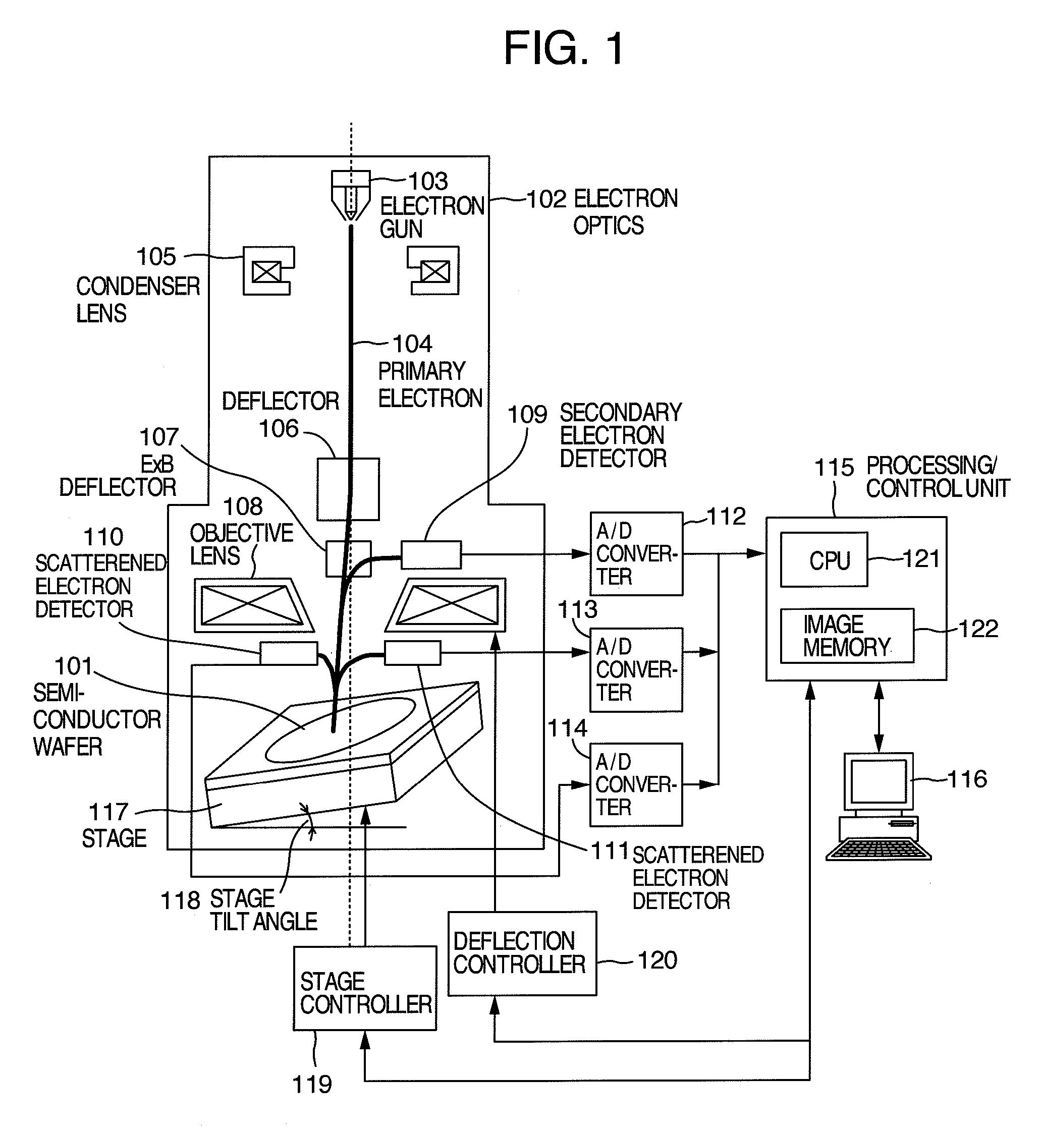
[0054] Referring first to FIG. 1, there is illustrated in block diagram form components constituting a scanning electron microscope (SEM) for acquiring a secondary electron image (SE image) or a backscattered electron image (BSE image) of a specimen in the embodiments of the invention. The SE image and the BSE image are generally termed an SEM image. An image acquired herein includes part or all of a top-down image of a measuring object observed in the vertical direction or of a tilt image of the object observed from a direction of arbitrary tilt angle.

[0055] An electron gun 103 emits an electron beam 104. The landing position of the electron beam and the aperture are controlled by means of a deflector 106 and an objective lens 108 such that the electron beam is focused and irradiated on an arbitrary position on a semiconductor wafer 101 repres...


PUM


Abstract

(1) part or all of the number, coordinates and size/shape and imaging sequence of imaging points each for observation, the imaging position change method and imaging conditions can be calculated automatically from CAD data, (2) a combination of input information and output information for imaging recipe creation can be set arbitrarily, and (3) decision is made of imaging or processing at an arbitrary imaging point as to whether to be successful/unsuccessful and in case a failure is determined, a relief process can be conducted in which the imaging point or imaging sequence is changed.

Description

INCORPORATION BY REFERENCE [0001] The present application claims priority from Japanese application JP2006-040125 filed on Feb. 17, 2006, the content of which is hereby incorporated by reference into this application. BACKGROUND OF THE INVENTION [0002] The present invention relates to a scanning electron microscope (SEM) capable of automatically imaging an arbitrary evaluation point on a specimen and a method therefore and more particularly, to an SEM apparatus having the function to create and determine an imaging recipe automatically from circuit design data without using an actual wafer and a method therefore, the imaging recipe being necessary for observing an arbitrary evaluation point with high image quality and high accuracy. Registered in the imaging recipe are imaging parameters such as coordinates of an imaging point, size / shape (of an imaging area associated the imaging point but will be simply referred to as imaging point size / shape in the following description), imaging...

Claims


Application Information

Patent Timeline
Patent Type & Authority Applications(United States)
IPC IPC(8): G21K7/00G03B42/00
CPCH01J37/21H01J37/265H01J37/28G01N23/20H01J2237/1536H01J2237/216H01J2237/2817H01J2237/1532
Inventor MIYAMOTO, ATSUSHINAGATOMO, WATARUMATSUOKA, RYOICHIMOROKUMA, HIDETOSHI
Owner HITACHI HIGH-TECH CORP
Why Eureka
Try Eureka