Semiconductor device and a method of increasing a resistance value of an electric fuse

a technology of a semiconductor device and an electric fuse, which is applied in the direction of semiconductor devices, semiconductor/solid-state device details, electrical apparatus, etc., can solve the problems of damage to the structure around the electric fuse, and achieve the effect of increasing reducing the time required for an increase in the resistance of the electric fus

Active Publication Date: 2007-09-13
RENESAS ELECTRONICS CORP
View PDF12 Cites 38 Cited by
  • Summary
  • Abstract
  • Description
  • Claims
  • Application Information

AI Technical Summary

Benefits of technology

[0016]According to this structure, heat from a central portion of the electric fuse does not diffuse outside easily since the electric fuse is meandering. Therefore, a structure around the electric fuse is restrained from being damaged by heat generated from the electric fuse. Moreover, a time required for an increase in the resistance of the electric fuse can be shortened since a large amount of heat is locally given only to the bent portion.
[0017]A different aspect of the invention is a method of increasing the resistance of an electric fuse wherein an electric current is supplied to the electric fuse which is any one of the above-mentioned electric fuses. In this way, the electric fuse is melted and is further cracked. Thereafter, apart of the melted electric fuse is absorbed into the crack by use of a capillary phenomenon. As a result, a discontinuous portion is formed in the electric fuse. According to this method, an electric fuse can be cut by a smaller electric current than that given to an electric fuse in any conventional method of using electromigration to cut the electric fuse.

Problems solved by technology

In such cases, a structure around the electric fuse may be damaged by heat generated from the fuse.

Method used


Image

  • Semiconductor device and a method of increasing a resistance value of an electric fuse
  • Semiconductor device and a method of increasing a resistance value of an electric fuse
  • Semiconductor device and a method of increasing a resistance value of an electric fuse

Examples


embodiment 1

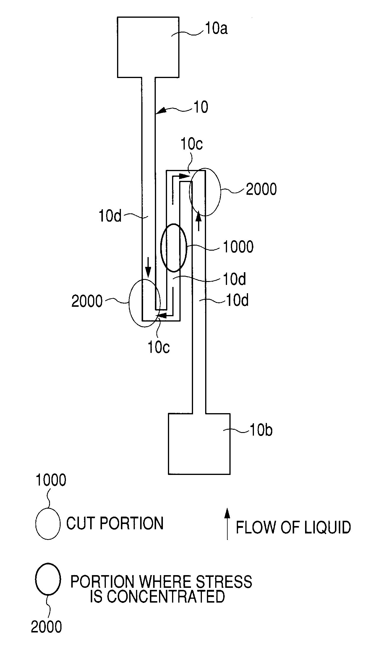
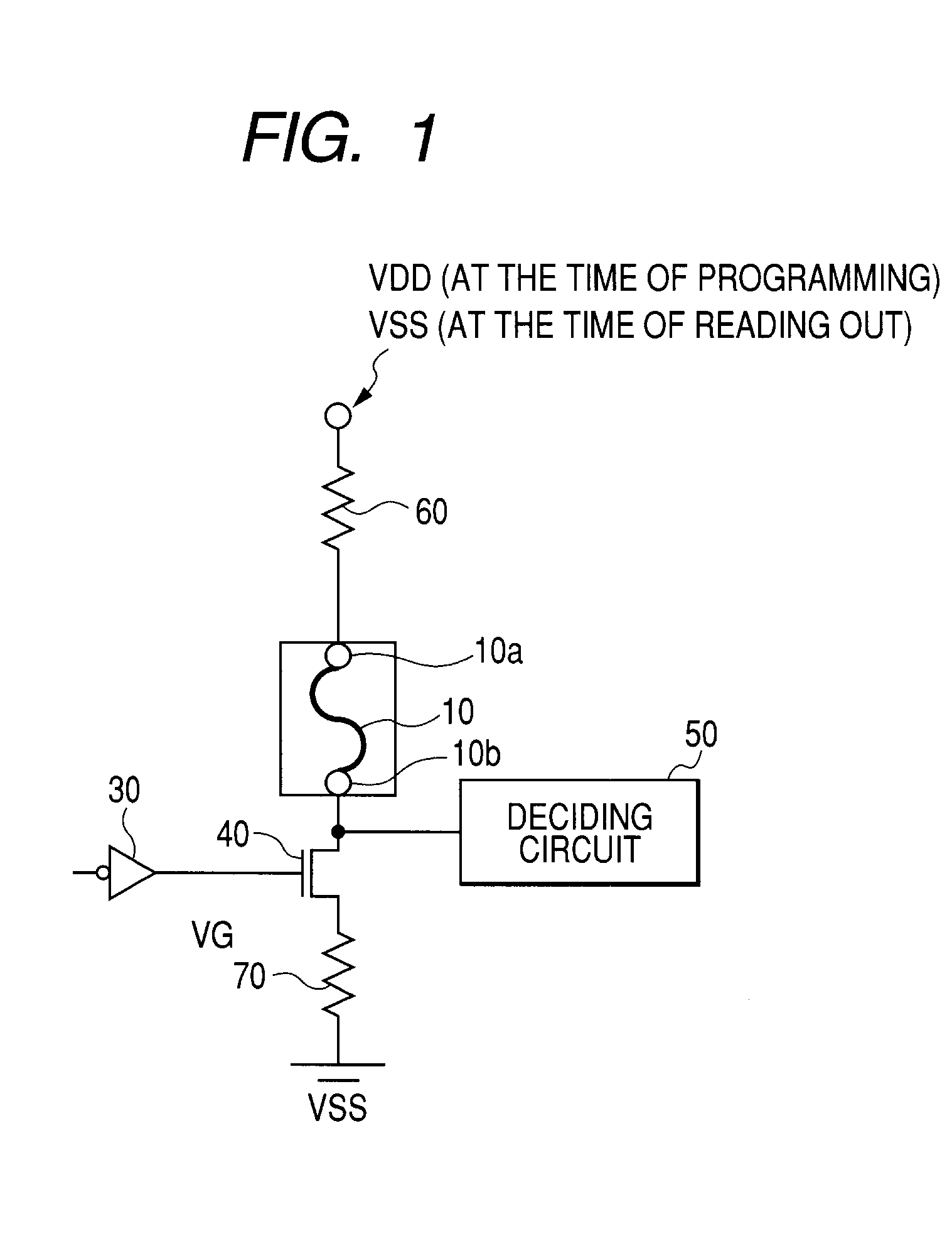
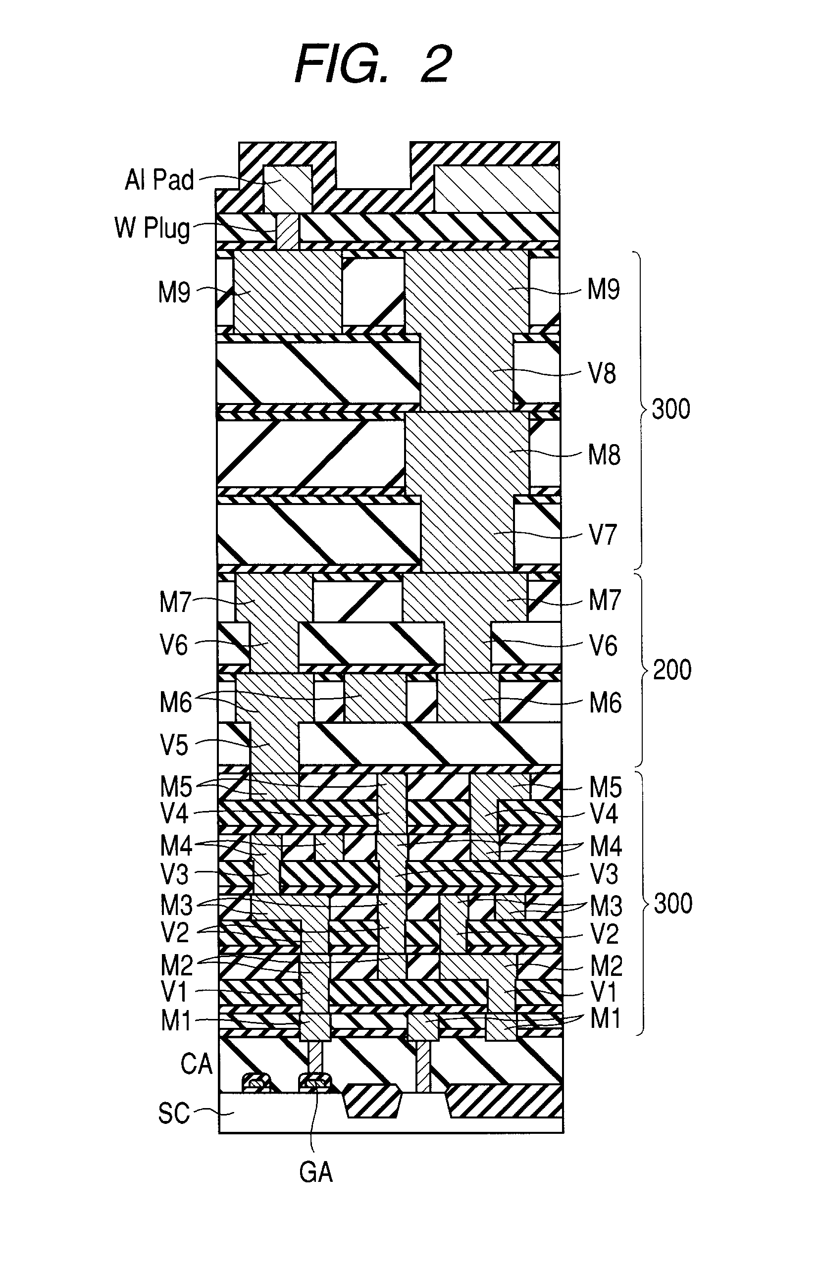
[0073]An electric fuse of an embodiment 1 of the present invention is not any electric fuse formed in the same layer in which a gate electrode is formed, as in the prior art. The electric fuse of the embodiment 1 is formed in a fine layer in a multi-layered structure including the fine layer, a semiglobal layer and a global layer in a semiconductor device. Therefore, the electric fuse is prevented from damaging its semiconductor substrate.

[0074]According to the structure of the semiconductor device of the embodiment 1, other elements, such as a transistor for controlling the flow of an electric current for increasing the resistance of the fuse, can be arranged in a space from the semiconductor substrate to the electric fuse; therefore, it is possible to make small the occupation area of elements arranged in a direction parallel to a main surface of the semiconductor substrate of the semiconductor device.

[0075]The increase in the resistance of the electric fuse of the embodiment 1 is...

embodiment 2

[0111]With reference to FIGS. 35 and 44, a method of an embodiment 2, wherein the resistance of an electric fuse is increased, is described herein. The electric fuse structure used in the embodiment 2 may be the same as in the embodiment 1.

[0112]In the embodiment 2, a method for cutting the electric fuse 10 described in the embodiment 1 more certainly is described. Specifically, described is a matter that it is necessary to adjust the rise time of electric pulses caused to flow into the electric fuse 10 in order to cut the electric fuse 10 more certainly.

[0113]When the electric fuse is cut, the temperature of the main wiring 1 needs to reach the melting point or a higher temperature. However, a phenomenon generated when the electric fuse 10 is cut is varied in accordance with the period from a time when a rise in the temperature of the main wiring 1 starts to a time when the temperature of the main wiring 1 reaches the melting point or a higher temperature. Accordingly, unless this ...

embodiment 3

[0135]With reference to FIGS. 45 to 47, a method of an embodiment 3, wherein the resistance of an electric fuse is increased, is described herein. The electric fuse structure in the embodiment 3 may be the same as in the embodiment 1.

[0136]In the case of using the method of increasing the resistance of an electric fuse according to each of the embodiments 1 and 2, the cracks 6 may not extend immediately in the insulator layer 4. This would be because a considerable large electric current cannot be caused to flow into the electric fuse 10 because of a problem resulting from the structure of the circuit and thus thermal stress generated in the electric fuse structure is not sufficiently large for generating the cracks 6. For this reason, the electric fuse 10 may not be cut by the cutting method described as the embodiment 1 or 2. Accordingly, a method for cutting the electric fuse 10 certainly in this case will be described hereinafter.

[0137]When an electric current is caused to flow ...


PUM


Abstract

Provided is a semiconductor device having an electric fuse structure which receives the supply of an electric current to be permitted to be cut without damaging portions around the fuse. An electric fuse is electrically connected between an electronic circuit and a redundant circuit as a spare of the electronic circuit. After these circuits are sealed with a resin, the fuse can be cut by receiving the supply of an electric current from the outside. The electric fuse is formed in a fine layer, and is made of a main wiring and a barrier film. The linear expansion coefficient of each of the main wiring and the barrier film is larger than that of each of the insulator layers. The melting point of each of the main wiring and the barrier film is lower than that of each of the insulator layers.

Description

CROSS-REFERENCE TO RELATED APPLICATION[0001]The present application claims priority from Japanese patent application No. 2006-256226 filed on Sep. 21, 2006, the content of which is hereby incorporated by reference into this application.BACKGROUND OF THE INVENTION[0002]The present invention relates to a semiconductor device which receives the supply of an electric current so as to be permitted to increase the resistance of the device itself, and a method of increasing the resistance of an electric fuse.[0003]Hitherto, there has been used a fuse which receives the supply of an electric current to be permitted to increase the resistance of the fuse itself. In the present specification, such a fuse is called an electric fuse. The electric fuse is set inside an insulator layer. In the specification, a structure having an insulator layer and an electric fuse is called an electric fuse structure. In the specification, an increase in the resistance of an electric fuse is, for example, a phe...

Claims


Application Information

Patent Timeline
Patent Type & Authority Applications(United States)
IPC IPC(8): H01L29/00H01L21/82
CPCH01L23/5256H01L2924/0002H01L2924/00H01L23/62H01H85/041H01L23/5227H01L23/525H01L23/528H01L23/5283H01L23/53228H01L23/53238H01L23/5329
Inventor IWAMOTO, TAKESHIKONO, KAZUSHIARAKAWA, MASASHIYONEZU, TOSHIAKIOBAYASHI, SHIGEKI
Owner RENESAS ELECTRONICS CORP
Why Eureka
Try Eureka