Metal-Induced Crystallization of Amorphous Silicon in Thin Film Transistors

a technology of thin film transistors and metal-induced crystallization, which is applied in the direction of semiconductor devices, basic electric elements, electrical appliances, etc., can solve the problems of inability to fully satisfy the requirements of the difficulty of using amorphous silicon tft for advanced applications

Inactive Publication Date: 2007-09-13
THE HONG KONG UNIV OF SCI & TECH
View PDF7 Cites 7 Cited by
  • Summary
  • Abstract
  • Description
  • Claims
  • Application Information

AI Technical Summary

Problems solved by technology

However, it has been difficult to use the amorphous silicon TFT for advanced applications such as liquid crystal displays having very high resolution.
There appears to be no presently available technique that can fully satisfy these requirements.

Method used


Image

  • Metal-Induced Crystallization of Amorphous Silicon in Thin Film Transistors
  • Metal-Induced Crystallization of Amorphous Silicon in Thin Film Transistors
  • Metal-Induced Crystallization of Amorphous Silicon in Thin Film Transistors

Examples


Embodiment Construction

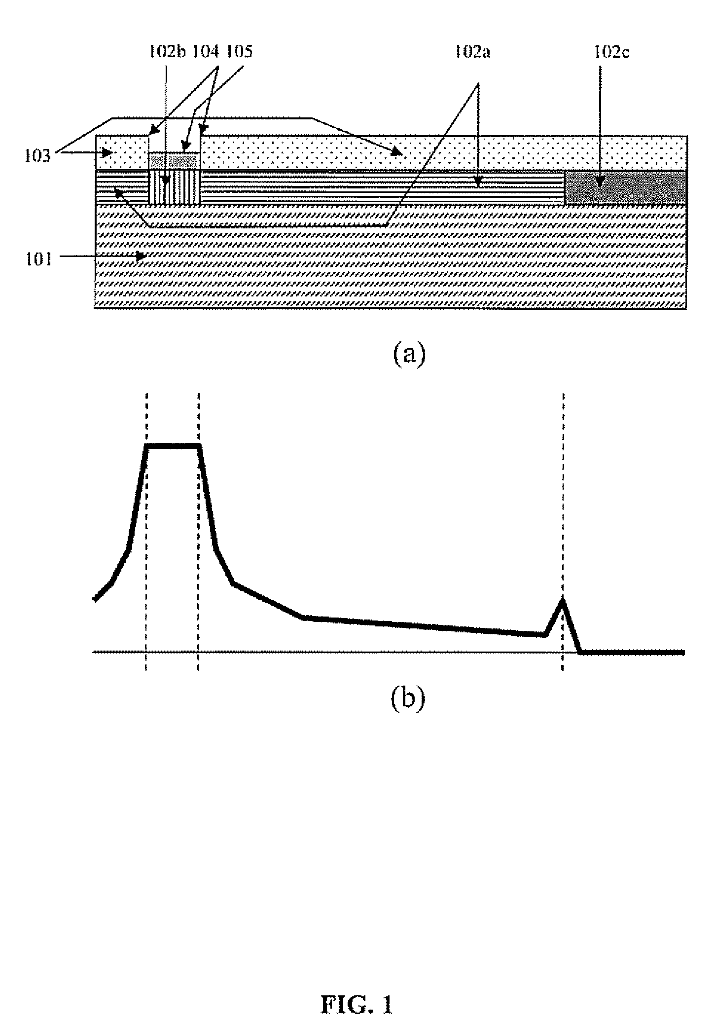
[0026]As shown in FIG. 1a, low temperature oxide (LTO) 103 is formed on an amorphous silicon film provided on substrate 101. The induced hole 104 is opened in a selected area in the LTO, and the nickel-containing layer 105 is formed on it. The sample is then annealed at 500-600° C. in a nitrogen atmosphere for several hours. At the same time, the metal induced crystallization area 102a, the metal induced lateral crystallization area 102b, and the non-crystallized area 102c are formed. As shown in FIG. 1b, the poly-Si near to induced hole contains a lot of nickel and cannot be used as active layer of TFT. So the high quality MILC area is only located in some appointed regions. Although the selected high quality MILC poly-Si film is suitable for TFTs with high electron mobility and low leakage current, alignment misplacement caused by the shrinkage of the substrate during the crystallization and the nickel gettering process is still not resolved. The present invention provides a metho...


PUM

PropertyMeasurementUnit
thicknessaaaaaaaaaa
thicknessaaaaaaaaaa
thicknessaaaaaaaaaa

Abstract

The invention provides a method for forming thin film transistors including a polycrystalline semiconducting film. The method comprises depositing a first layer of amorphous semiconducting thin film on to a substrate; depositing a second layer of thin film on to the first layer of amorphous semiconducting thin film; patterning the second layer or thin film so that the first layer of amorphous semiconducting thin film is exposed at selected locations; exposing the first and second layers of thin film to a nickel containing compound in either a solution or a vapor phase; removing the second layer of thin film; and annealing the first layer of amorphous semiconducting thin film at an elevated temperature so the first layer of amorphous semiconducting thin film converts into a polycrystalline semiconducting thin film.

Description

[0001]This application claims priority of U.S. Provisional Patent Application No. 60 / 781,496, filed Mar. 13, 2006 and U.S. Provisional Patent Application No. 60 / 838,807, filed on Aug. 18, 2006. The entire contents of these applications are incorporated herein by reference.FIELD OF THE INVENTION[0002]The present invention relates to thin film transistors using low temperature polycrystalline silicon. In particular, the invention provides a polycrystalline layer in a thin film transistor using the technique of patterned crystallization with the assistance of metal impurities.BACKGROUND OF THE INVENTION[0003]To obtain high quality flat panel displays, active-matrix driving technology is needed. This includes liquid crystal displays (LCDs) and organic light emitting diodes (OLEDs). Active matrix driving allows full color realization and high resolution without cross-talk. The key technology of active-matrix driving display involves the fabrication of thin film transistors (TFTs) on a su...

Claims


Application Information

Patent Timeline
Patent Type & Authority Applications(United States)
IPC IPC(8): H01L21/20
CPCH01L21/02422H01L27/1277H01L21/02672H01L21/02532
Inventor KWOK, HOI SINGWONG, MANMENG, ZHIGUOZHAO, SHUYUNWU, CHUNYA
Owner THE HONG KONG UNIV OF SCI & TECH
Why Eureka
Try Eureka