Solid-state imaging device and imaging apparatus

a solid-state imaging and imaging apparatus technology, applied in the field of solid-state imaging devices, can solve the problems of reducing the light collection amount at the photodiodes, deteriorating image quality, and reducing the light-receiving area in each unit pixel, so as to reduce the number of transistors and wiring

Active Publication Date: 2007-09-20
SONY SEMICON SOLUTIONS CORP
View PDF3 Cites 64 Cited by
  • Summary
  • Abstract
  • Description
  • Claims
  • Application Information

AI Technical Summary

Benefits of technology

[0025]As an example of the above, it is possible to form a CMOS image sensor, as described later with reference to FIG. 1 to 3 in Embodiment 1 of the invention, in which an FD region 4 which is common to two or four unit

Problems solved by technology

If light leaks into a circuit unit formed by the MOS transistors, photoelectric conversion occurs and a pseudo signal is generated by electrons thus generated, which becomes noise.
Accordingly, in a solid-state imaging apparatus which takes images by focusing a subject by a lens, there is a problem that shading is large in a region near the periphery of an imaging area, that is, a problem that light entering obliquely is shielded by the shielding film or wiring, consequently, the amount of light collected at the photodiodes

Method used


Image

  • Solid-state imaging device and imaging apparatus
  • Solid-state imaging device and imaging apparatus
  • Solid-state imaging device and imaging apparatus

Examples


embodiment 1

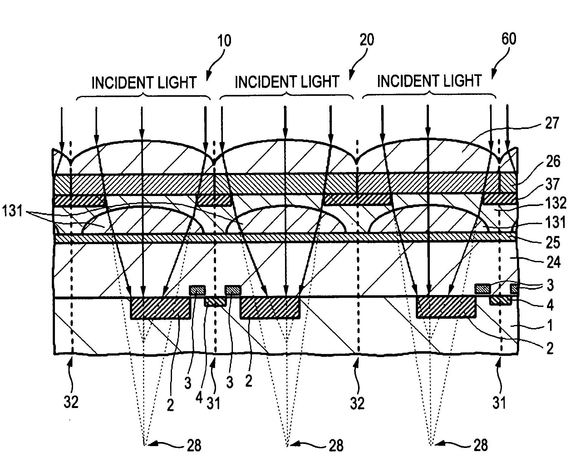
[0068]In Embodiment 1, as an example of the solid-state imaging device of the invention, a CMOS image sensor will be explained. In the CMOS image sensor, an FD (floating diffusion) region common to two or four unit areas (hereinafter, referred to as unit pixels) is provided as an output extraction region which is common to the plural photoelectric conversion regions, and an amplifying transistor, a vertical selecting transistor and a reset transistor are shared between these unit pixels, thereby reducing the number of transistors at each unit pixel to sufficiently secure the light receiving area of the photodiode.

[0069]As a result of the above, it is inevitable that the photoelectric conversion region is provided being deviated from the central position of each unit pixel. In order to respond to this, in Embodiment 1, a high refractive index material layer is arranged over the deviated photoelectric conversion regions as well as a low refractive index material layer is arranged over...

embodiment 2

[0089]In Embodiment 2, as an example of the solid-state imaging device of the invention, a CMOS image sensor will be explained.

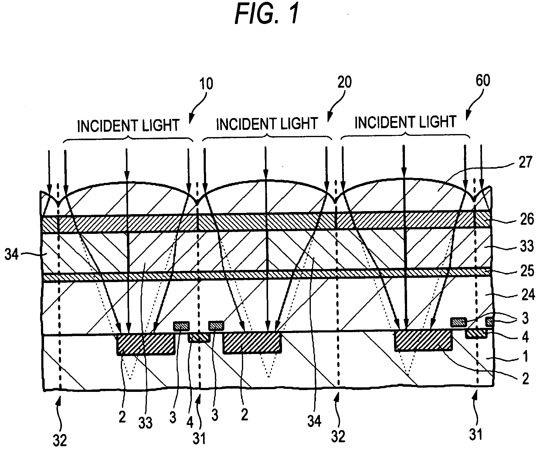
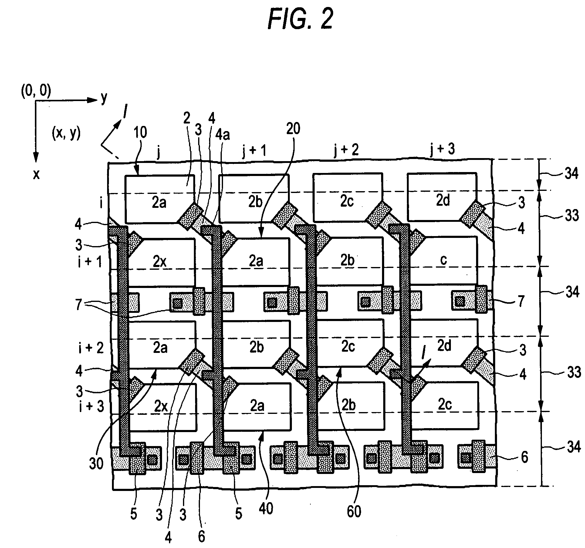
[0090]In the CMOS image sensor, as same as Embodiment 1, the FD region which is common to two or four unit areas (hereinafter, referred to as unit pixels) is provided as the output extraction region common to the plural photoelectric conversion regions, and the amplifying transistor, the vertical selecting transistor and the reset transistor are shared between the unit pixels, thereby decreasing the number of transistors at each unit pixel to sufficiently secure the light receiving area of photodiodes (refer to FIG. 2).

[0091]As a result, it is inevitable that the photoelectric conversion region is provided being deviated from the central position of each unit pixel. In order to respond to this, in Embodiment 2, one or plural lenses are provided along light paths of incident light over the deviated photoelectric conversion regions, and at least one of them is...

embodiment 3

[0106]FIG. 5 is a block diagram showing a configuration of an imaging apparatus based on Embodiment 3 of the invention. The imaging apparatus includes, in addition to the CMOS image sensor described in Embodiment 1 or 2 as a solid-state imaging element (solid-state imaging device) 42, a lens 41, an imaging circuit unit 43 which performs imaging processing based on a control signal from an AE (auto exposure) calculation / control unit 45, a timing generator 47 which controls the timing of the solid-state imaging element 42 and the AE calculation / control unit 45, an integration 48 which analyses a signal outputted from the imaging circuit unit 43 and the control signal from the AE calculation / control unit 45, a signal processing unit 44 which processes the signal outputted from the imaging circuit unit 43 using a control signal generated in an AWB (auto white balance) calculation / control unit 46 based on the signal from the integration 48, a display unit 49 which displays the signal out...


PUM


Abstract

A solid-state imaging device is disclosed. In the solid-state imaging device, plural unit areas, each having a photoelectric conversion region converting incident light into electric signals are provided adjacently, in which each photoelectric conversion region is provided being deviated from the central position of each unit area to a boundary position between the plural unit areas, a high refractive index material layer is arranged over the deviated photoelectric conversion region, and a low refractive index material layer is provided over the photoelectric conversion regions at the inverse side of the deviated direction being adjacent to the high refractive index material layer, and optical paths of the incident light are changed by the high refractive index material layer and the low refractive index material layer, and the incident light enters the photoelectric conversion region.

Description

CROSS REFERENCE TO RELATED APPLICATIONS[0001]The present invention contains subject matter related to Japanese Patent Application JP 2006-076693 filed in the Japanese Patent Office on Mar. 20, 2006, the entire contents of which being incorporated herein by reference.BACKGROUND OF THE INVENTION[0002]1. Field of the Invention[0003]The present invention relates to a solid-state imaging device having a photoelectric conversion means and the like, particularly, relates to a solid-state imaging device and an imaging apparatus including an optical path changing means.[0004]2. Description of the Related Art[0005]Recently, video cameras and electronic cameras are widely used. In these cameras, an amplifying solid-state imaging device such as a CCD (Charge Coupled Device) solid-state imaging device or a CMOS (Complementary Metal Oxide Semiconductor) image sensor is used. In an imaging unit of the solid-state imaging device, plural photoelectric conversion regions formed by photo diodes are ar...

Claims


Application Information

Patent Timeline
IPC IPC(8): H01L31/112G02B5/13H01L27/14H04N5/3745
CPCH01L27/14603H01L27/14609H01L27/14641H01L27/14627H01L27/14623
Inventor KIDO, HIDEOISHIWATA, HIROAKI
Owner SONY SEMICON SOLUTIONS CORP
Why Eureka
Try Eureka