
Semiconductor package with enhancing layer and method for manufacturing the same

a technology of enhancing layer and semiconductor, applied in the field of semiconductor package, can solve the problems of unsolved problems in fcqfn package, large difference in thermal expansion coefficient between the chip and the leadframe, and bumps that collapse after packaging, etc., to achieve enhanced mechanical strength of bumps, prevent collapsing, and easy electroplating

Inactive Publication Date: 2007-09-20
ADVANCED SEMICON ENG INC
View PDF23 Cites 6 Cited by
  • Summary
  • Abstract
  • Description
  • Claims
  • Application Information

AI Technical Summary

Benefits of technology

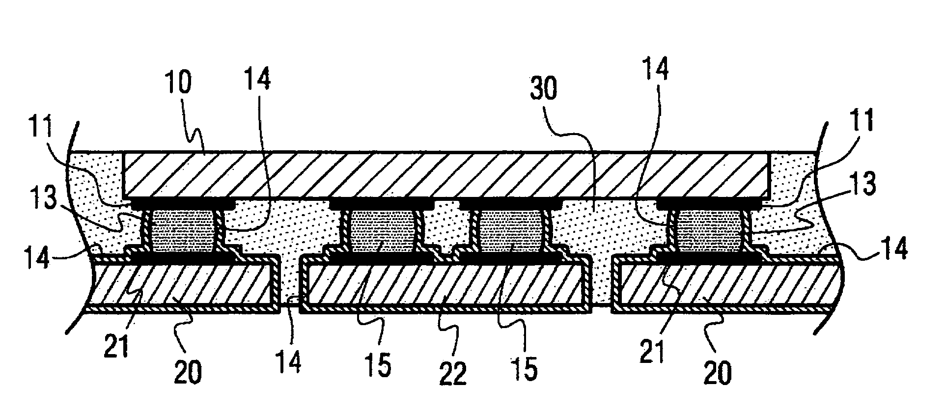
[0013]Therefore, in a FCQFN package of the present invention, copper or another metal with thickness about 10-30 μm is easily electroplated on the bumps and in other regions of the package because the space around the bumps after flip-chip step is large enough. The advantages are as follow. First, the mechanical strength of the bumps is enhanced. The method can also be applied to general eutectic solder bumps. Second, the bumps are prevented from collapsing at high temperature. The melting point of copper is high, so that most of the currency flows through the surfaces of the bumps when high frequent signals are transmitted. As a result, the conductivity is increased greatly. Third, the problem of high resistance in flip chip packages with gold stud bumps adhered to silver paste is solved. Therefore, the packages of the present invention are suitable for products with high frequency.
[0014]The conventional packaging problems due to the material properties are solved. Chips are prevented from moisture and heat. Besides, chips are electrically connected to an outer circuit effectively to achieve the goal of chip packaging.

Problems solved by technology

However, there are still some unsolved problems in FCQFN packages.
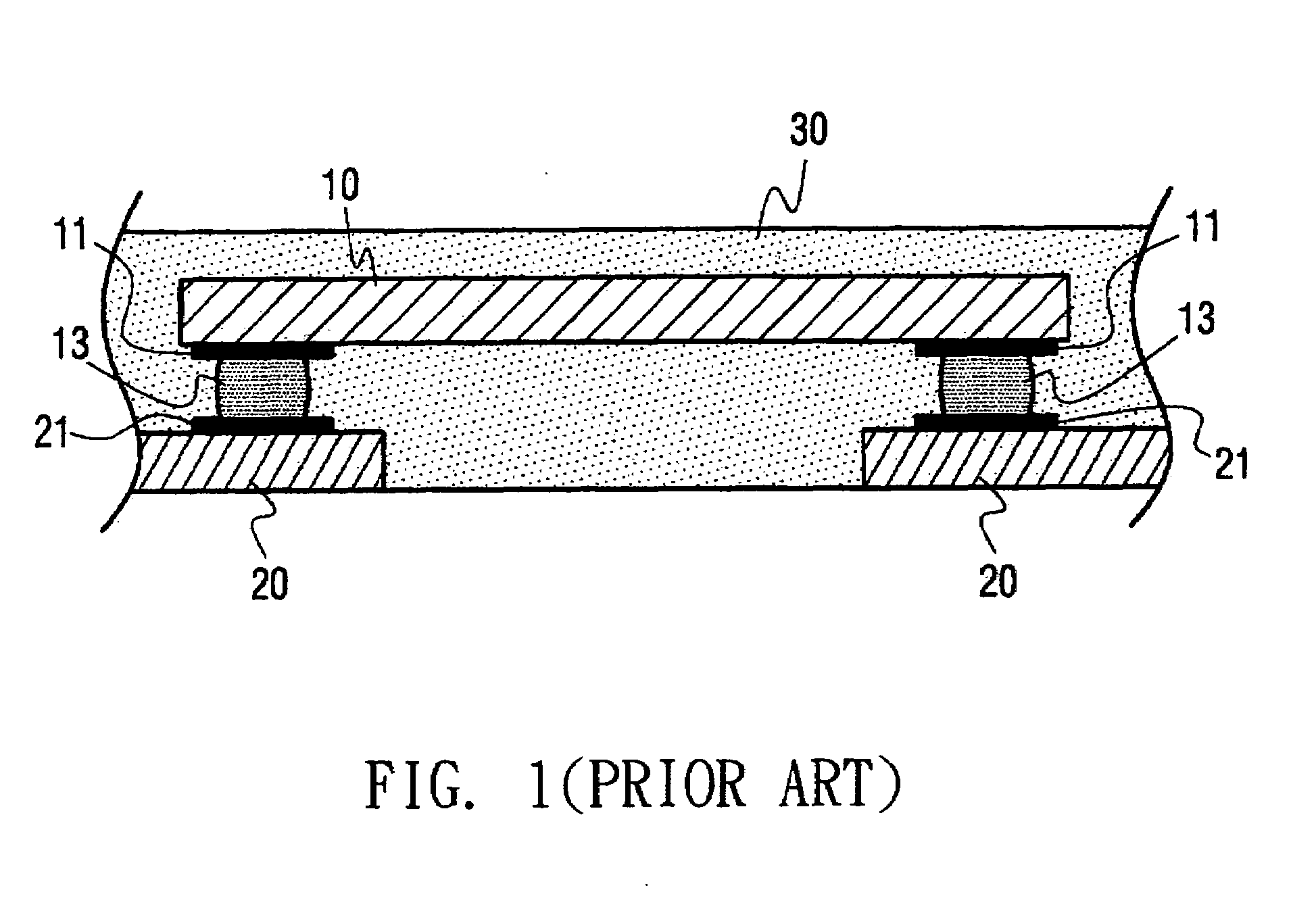
Furthermore, because the reflowing temperature of lead-free and high-lead bumps is too high, difference of thermal expansion coefficient between the chip and the leadframe is so large that the bumps collapse after packaging.
Therefore, the chips are affected by moisture and heat and not electrically connected to an outer circuit effectively.
The chips are not sufficiently protected through the packaging process.
Accordingly, FCQFN packages have problems including bump collapse and huge difference of thermal expansion coefficient between the chip and the frame.
After a reliability experiment, collapse occurs between the frame and the conductive silver paste because the silver paste can not bear strong stress.
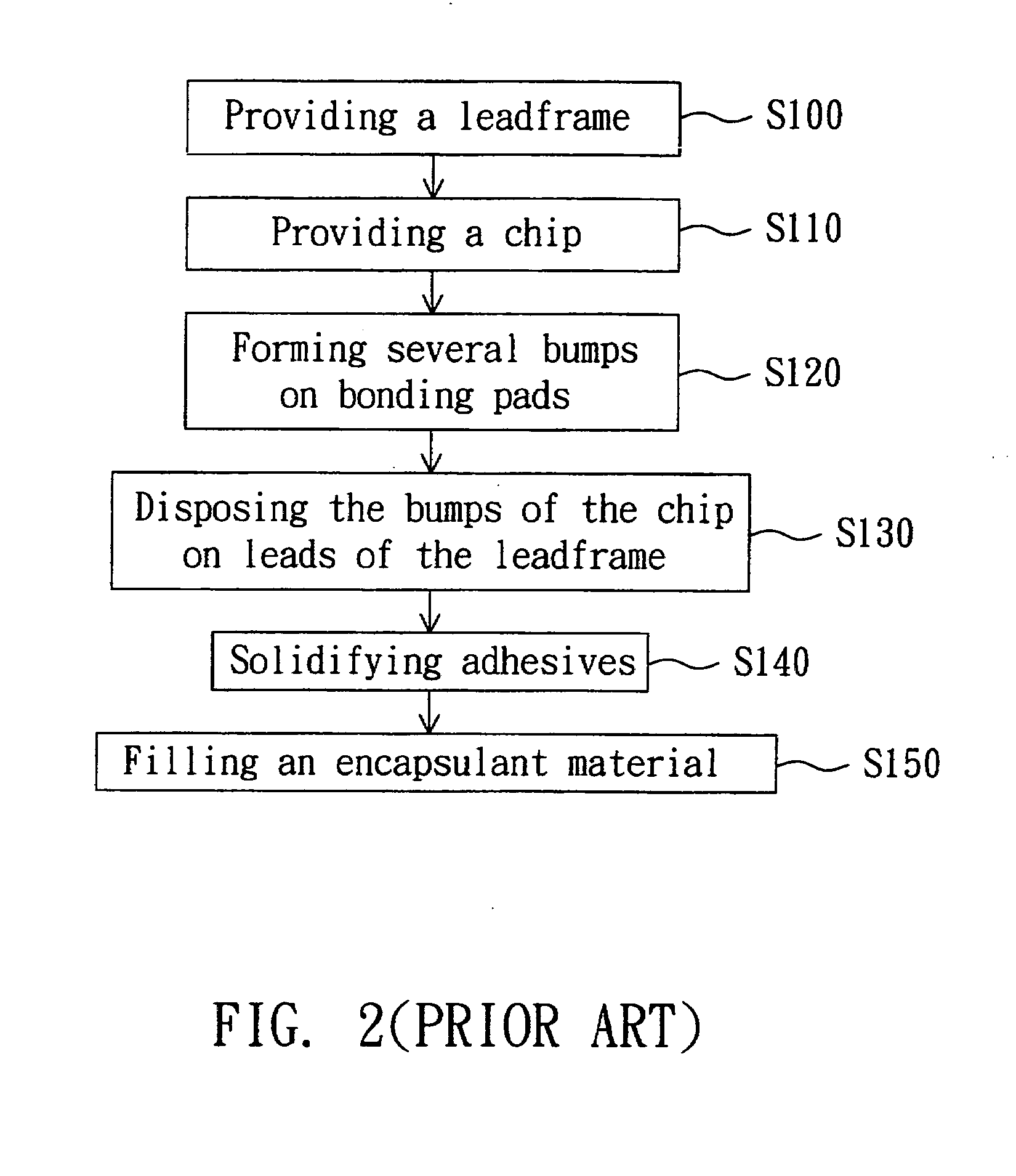
However, there are still some unsolved problems due to material properties in the above method for manufacturing a semiconductor package.
Also, because the reflowing temperature of lead-free and high-lead bumps is too high, the difference of thermal expansion coefficient between the chip and the frame is so large that the bumps collapse after packaging.
Therefore, the chips are affected by moisture and heat and not electrically connected to an outer circuit effectively.
The chips are not sufficiently protected through the packaging process.
Hence, there are still a lot of problems to be solved in the conventional packaging technology.

Method used


Image

  • Semiconductor package with enhancing layer and method for manufacturing the same
  • Semiconductor package with enhancing layer and method for manufacturing the same
  • Semiconductor package with enhancing layer and method for manufacturing the same

Examples


Embodiment Construction

[0021]Please referring to FIG. 3A, a semiconductor package with an enhancing layer according to a preferred embodiment of the invention is illustrated in FIG. 3A. The semiconductor package includes a leadframe 20, a chip 10 several bumps 13, an enhancing layer 14 and an encapsulant material 30. The leadframe 20 includes several leads 21. Several bonding pads 11 are disposed on a surface of the chip 10. The bumps 13 connect the bonding pads 11 of the chip 10 and the leads 21 of the leadframe 20. The bumps 13 are composed of gold, copper, lead, fin or silver. The bumps 13 further include several conductive adhesives. The conductive adhesives are composed of lead, tin, copper or silver.

[0022]The enhancing layer 14 preferably covers the leads 21 and the bumps 13. Or, the enhancing layer 13 covers only the conductive adhesives of the bumps 13. The enhancing layer 14 is made of metal and preferably a continuous metal layer. The enhancing layer 14 connects the bumps 13 and the leads 21. Mo...


PUM


Abstract

A semiconductor package with an enhancing layer is provided. The package includes a leadframe, a chip, several bumps and an enhancing layer. The leadframe includes several leads. Several bonding pads are disposed on a surface of the chip. The bumps connect the bonding pads of the chip and the leads of the leadframe. The enhancing layer covers the leads and the bumps. The enhancing layer including copper is formed by electroplating. Or, the melting point of the enhancing layer is greater than the melting points of lead and tin.

Description

[0001]This application claims the benefit of Taiwan application Serial No. 95108840, filed Mar. 15, 2006, the subject matter of which is incorporated herein by reference.BACKGROUND OF THE INVENTION[0002]1. Field of the Invention[0003]The invention relates in general to a semiconductor package and a method for manufacturing the same, and more particularly to a semiconductor package with an enhancing layer and a method for manufacturing the same.[0004]2. Description of the Related Art[0005]Recently, portable terminal products, such as notebooks, mobile phones, personal digital assistants and digital camera, have become a main trend in the market. Considerable efforts have been made to minimize the volume and weight of portable terminal products. Take mobile phones for example. Under the demand for minimizing the volume and weight, chips are developed in coordination with electronic devices to be digital, high processing speed, multi-functional and miniaturized.[0006]According to the a...

Claims


Application Information

Patent Timeline
Patent Type & Authority Applications(United States)
IPC IPC(8): H01L23/02
CPCH01L21/568H01L23/3107H01L23/4334H01L2924/01322H01L23/49582H01L2224/16H01L2924/01079H01L23/49568H01L2224/05568H01L2224/05573H01L2924/00014H01L2224/05599
Inventor CHEN, HUI-PINHU, CHIA-CHIEH
Owner ADVANCED SEMICON ENG INC
Learn More