Display device and method of manufacturing display device
a display device and display device technology, applied in the field of display devices, can solve the problems of display quality deterioration, display unevenness of display images, monomer unpolymerization, etc., and achieve the effect of reducing resistance, reducing increasing resistance, and reducing appearance quality
- Summary
- Abstract
- Description
- Claims
- Application Information
AI Technical Summary
Benefits of technology
Problems solved by technology
Method used
Image
Examples
first embodiment
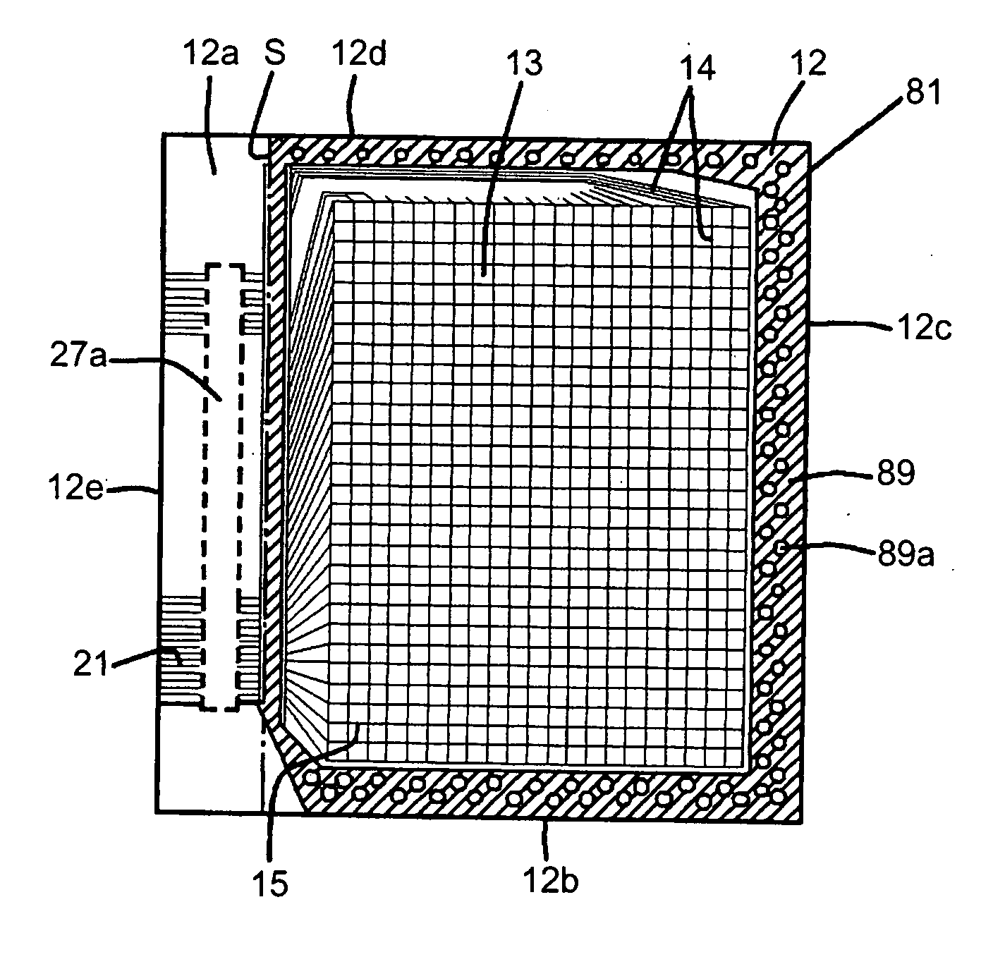
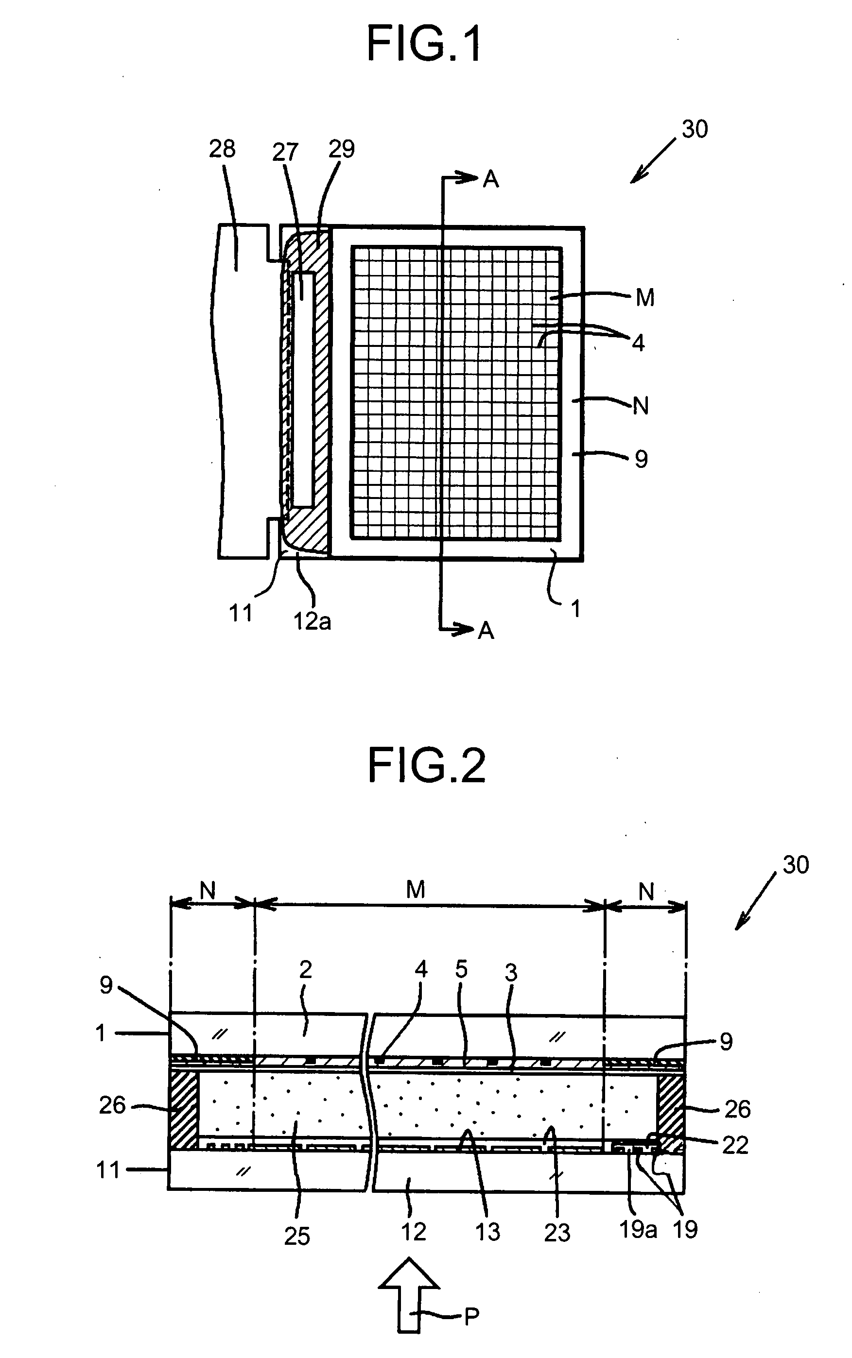
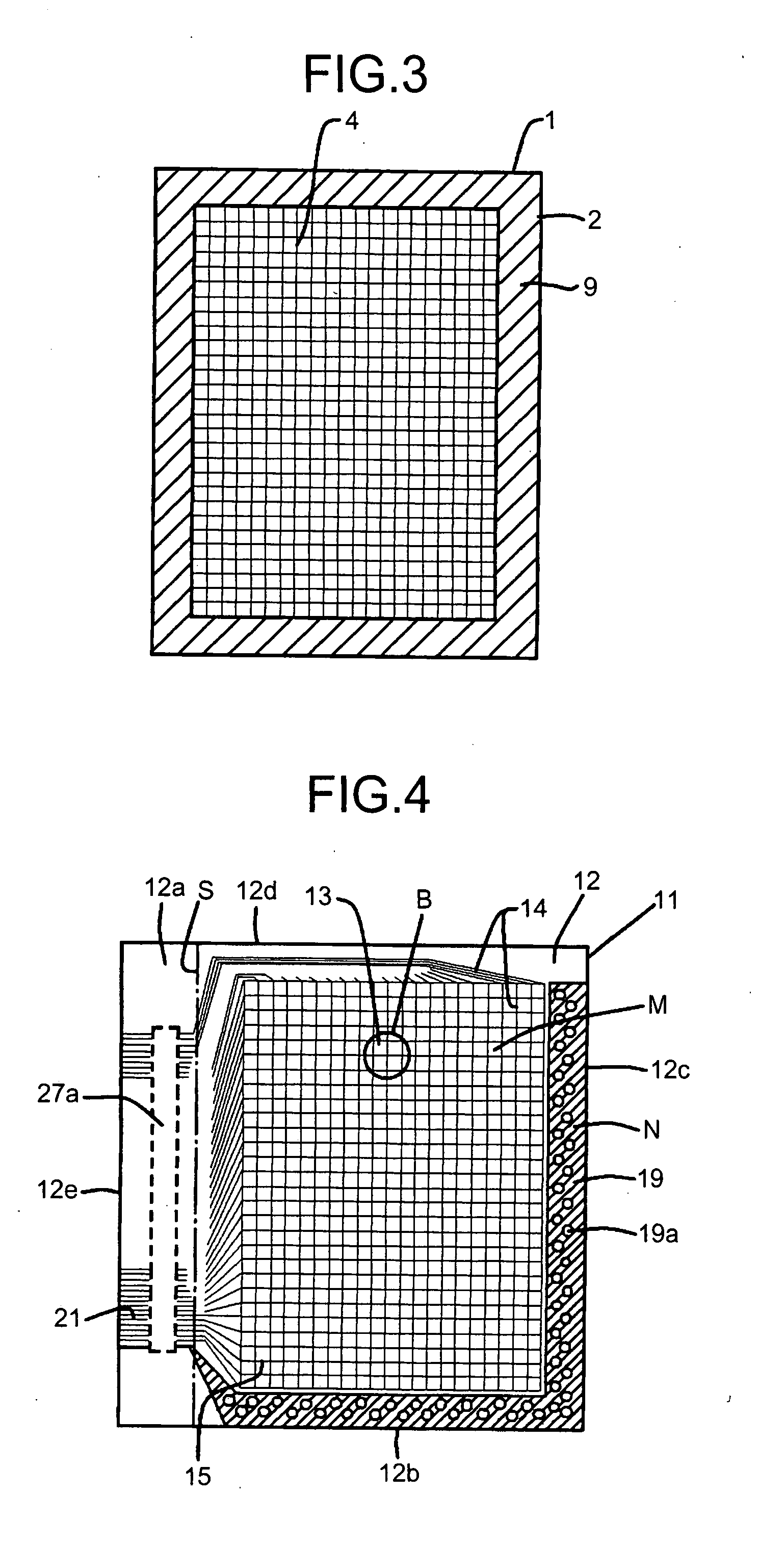
[0070] A display apparatus 30 according to the present invention is a display apparatus that uses a liquid crystal, and has a structure where a polymer dispersed liquid crystal material 25 is encapsulated in a gap between a completed first substrate 1 and a completed second substrate 11 arranged to face each other by using a sealing member 26 as depicted in FIG. 2. As shown in FIG. 1, the completed second substrate 11 has an extended portion 12a on one side thereof and is formed to be larger than the completed first substrate 1, and a liquid crystal driving IC 27 and a circuit substrate 28 as an FPC are provided on the extended portion 12a. This display apparatus 30 has an active matrix type display configuration. Although not depicted in FIG. 2, a transparent spacer, e.g., silica particles or plastic particles is dispersedly arranged between the completed first substrate 1 and the completed second substrate 11 to assure a necessary gap amount.
[0071] As shown in FIGS. 1 and 2, M den...
second embodiment
[0102] The wiring electrode 39 is formed of an aluminum (Al) metal film, and arranged with a necessary gap L from the display region M as depicted in FIG. 8. This gap L forms an ultraviolet ray transmitting portion, and a monomer that is present in a region of the light shielding member 9 (e.g., the peripheral region N) is irradiated with an ultraviolet ray from this gap L. The transparent electrode 42 arranged on the wiring electrode 9 is provided to overlap the wiring electrode 39 and enter the region of the gap L. This wiring electrode 39 is connected with the first transparent electrode 3 of the completed first substrate 1 via electroconductive particles mixed in the sealing member 26, thereby achieving electrical conduction with respect to the first transparent electrode 3 from the wiring electrode 39. The wiring electrode 39 is provided to reduce a wiring resistance with respect to the first transparent electrode 3, and formed of an aluminum (Al) metal film. Since the transpa...
third embodiment
[0114] the light shielding member 59 is formed of a two-layered metal film including a chrome oxide (CrO) metal film and a chrome (Cr) metal film like the black matrix 4. Since the light shielding member 59 having the second small holes 59a provided therein is formed of the same material as that of the black matrix 4, the light shielding member 59 having the small holes 59a provided therein and the black matrix 4 are simultaneously formed. A method of forming the light shielding member 59 having the second small holes 59a provided therein and the black matrix 4 is as follows. First, a chrome oxide (CrO) metal is first formed with a necessary thickness on an entire surface of the completed first substrate 51 on the second substrate 2 side by, e.g., a vacuum deposition method, a sputtering method, or an ion-plating method. Then, a chrome (Cr) metal film is formed on the chrome oxide (CrO) metal film by the same method. For example, when the vacuum deposition method is adopted, a pres...
PUM
| Property | Measurement | Unit |
|---|---|---|
| thickness | aaaaa | aaaaa |
| temperature | aaaaa | aaaaa |
| particle diameter | aaaaa | aaaaa |
Abstract
Description
Claims
Application Information


