Nitride semiconductor laser element and method for manufacturing same

Active Publication Date: 2007-09-20
NICHIA CORP
View PDF5 Cites 22 Cited by
  • Summary
  • Abstract
  • Description
  • Claims
  • Application Information

AI Technical Summary

Benefits of technology

[0023]With the nitride semiconductor laser element of the present invention, a cavity (or gap) is formed on both sides of a ridge, which effectively minimizes the stress applied to the interface between a first protective film and the ridge, and also extends the service life characteristics. In addition, this cavity stabilizes optical confinement. This is not limited to a single-mode nitride semiconductor laser element, and can also be employed in multi-mode nitride semiconductor laser elements. Furthermore, because control of the horizontal lateral mode is possible when the present invention is applied to a single-mode nitride semiconductor laser element, the threshold can be lowered, and a further decrease in power usage can be achieved.
[0024]Also, with the method of the present invention for manufacturing a nitride semiconductor laser element, a cavity can be formed with good control on both sides of a ridge, making it possible to manufacture a high-performance nitride semiconductor laser element in a simple way.

Problems solved by technology

Also, it was difficult to control optical confinement in the horizontal-lateral mode because it affected the adhesion and thickness of the protective film formed on the semiconductor laser on both sides of the ridge.
With the structure described in Japanese Laid-Open Patent Application H10-270792, for example, the embedding layer is formed in a thickness that is equal to the height of the upper surface of the ridge from the exposed part of the semiconductor laser, so a difference in the coefficients of thermal expansion between the semiconductor laser and the embedding layer may result in interfacial separation between the embedding layer and the semiconductor laser, which leads to current leakage.
There is also the danger that cracks will develop in the embedding layer and that current will leak from these cracks.
With the semiconductor laser element described in Japanese Laid-Open Patent Application 2005-166718, there is an cavity on the outside of the dielectric film formed on the side faces of the ridge, so lateral mode control is unlikely to be possible.
Furthermore, since this semiconductor laser element is a GaAs-based semiconductor element, it has an eave-like shape, but with a nitride semiconductor the ridge shape tends to be difficult to form in an eave shape.
Also, with a configuration in which a gap is enclosed by a dielectric film, a large current is required, and with a GaN-based semiconductor element that is prone to generating heat, its operation over time results in stress being applied between the gap and the dielectric film.
Consequently, separation tends to occur at the interface between the two, the gap itself becomes unstable, and this causes the operating current to be unstable, making it impossible to control optical confinement.

Method used


Image

  • Nitride semiconductor laser element and method for manufacturing same
  • Nitride semiconductor laser element and method for manufacturing same
  • Nitride semiconductor laser element and method for manufacturing same

Examples


example 1

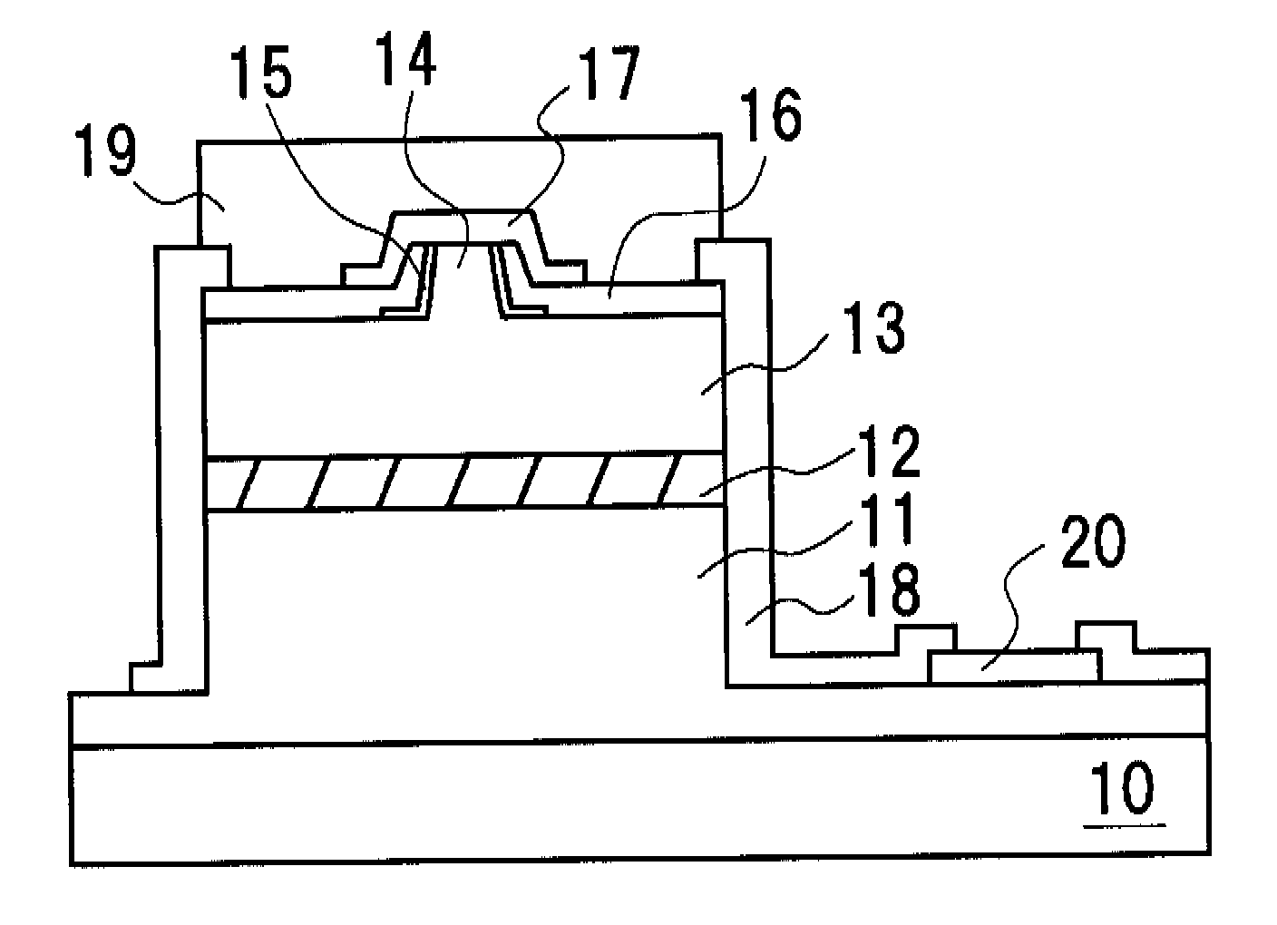
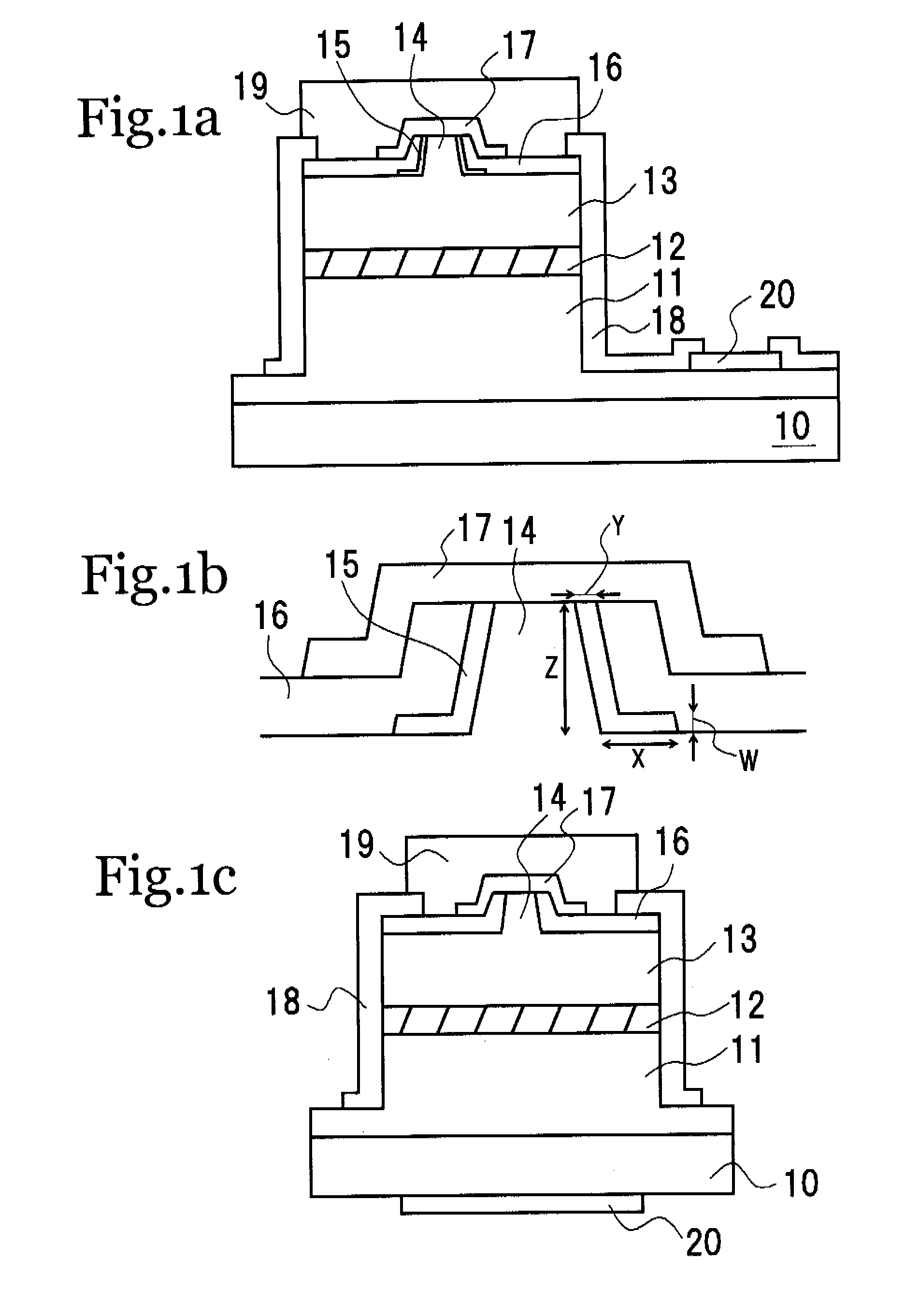
[0084]The laser element in this example oscillates in a band of 390 nm and under, and as shown in FIGS. 1a and 1b, a first buffer layer (100 nm) composed of silicon-doped Al0.02Ga0.98N and a second buffer layer (150 nm) composed of silicon-doped In0.1Ga0.9N are formed on a substrate 10 composed of n-type GaN. Over this, an n-side cladding layer (0.7 μm) composed of silicon-doped Al0.11Ga0.89N and an n-side light guide layer (0.15 μm) composed of undoped Al0.06Ga0.94N are formed as an n-side semiconductor layer 11, and a barrier layer (7 nm) composed of silicon-doped Al0.15Ga0.85N, a well layer (10 nm) composed of undoped In0.01Ga0.09N, and a barrier layer (5 mm) composed of Al0.15Ga0.85N are formed as an active layer 12 composed of a single quantum well. Over this are formed a p-side cap layer (10 nm) composed of magnesium-doped p-side Al0.30Ga0.70N, a p-side light guide layer (0.15 μm) composed of undoped Al0.06Ga0.94N, a p-side cladding layer composed of a superlattice layer with ...

example 2

[0106]Substantially the same element as in Example 1 is formed in the same way, except that in this example the first protective film has a two-layer structure with ZrO2 of different film quality.

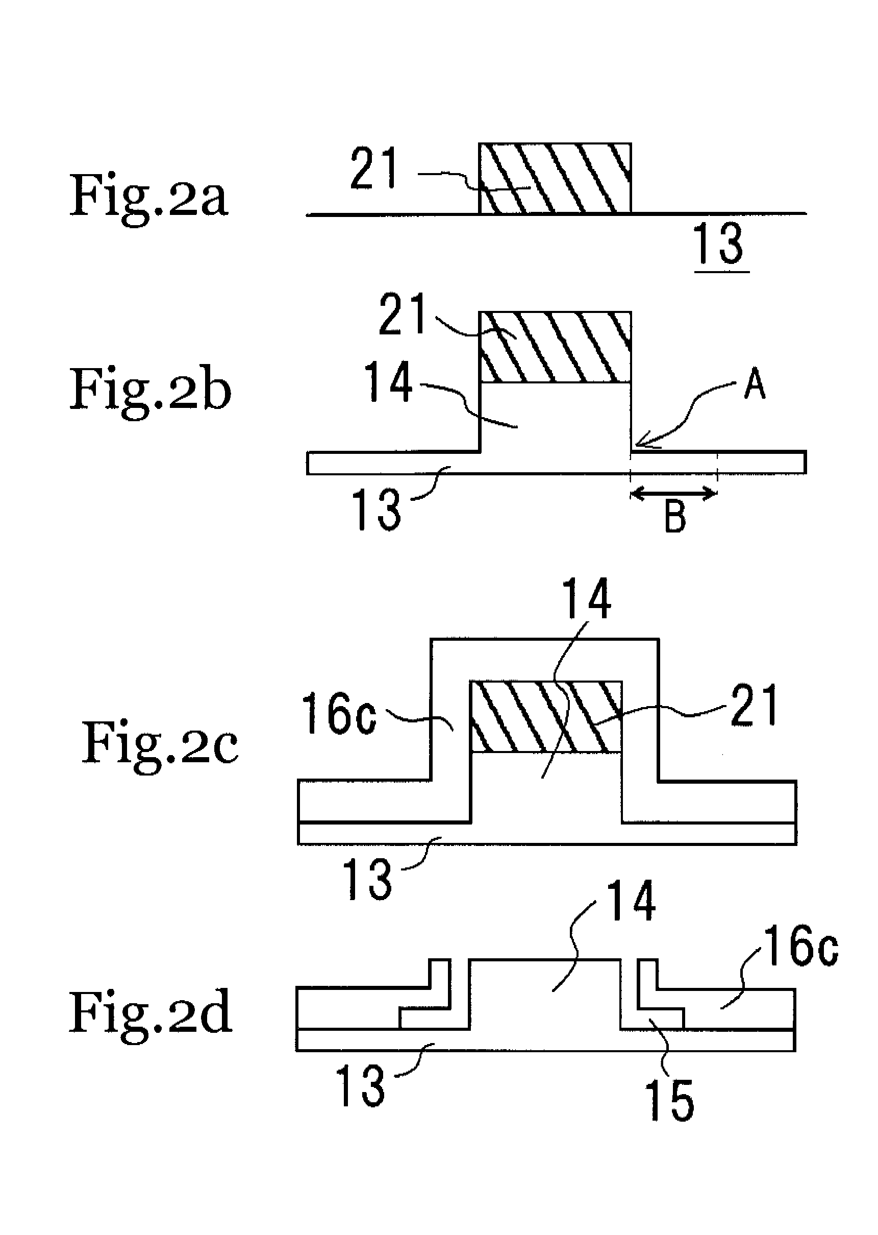
[0107]First, just as in Example 1, a ridge is formed on the nitride semiconductor layer surface using a mask pattern, and as shown in FIG. 3a, a ZrO2 film with a thickness of 10 nm is formed as a lower layer 16a of the first protective film using a magnetron sputtering device. Next, a ZrO2 film with a thickness of 90 nm is formed as an upper layer 16b using an ECR sputtering device.

[0108]The first protective films 16a and 16b thus obtained are annealed at 300° C. and immersed in BHF for 15 minutes, which, as shown in FIG. 3b, dissolved away the mask pattern formed on the p-side contact layer, and the first protective film on the p-side contact layer is removed along with the mask pattern by lift-off method. Further, a cavity is formed in this step by etching the lower layer 16a and upper la...

example 3

[0110]Substantially the same element as in Example 1 is formed in the same way, except that in this example the first protective film has a two-layer structure composed of different materials.

[0111]First, just as in Example 1, a ridge is formed on the nitride semiconductor layer surface using a mask pattern, and an SiO2 film with a thickness of 10 nm is formed as the lower layer of the first protective film using an ECR sputtering device. Next, a ZrO2 film with a thickness of 40 nm is formed as the upper layer using an ECR sputtering device.

[0112]The first protective film thus obtained is annealed at 400° C. and immersed in BHF for 15 minutes, which dissolved away the mask pattern formed on the p-side contact layer, and the first protective film on the p-side contact layer is removed along with the mask pattern by lift-off method. Further, a cavity is formed in this step at the ridge side faces and the ridge bottom face by etching the SiO2 film serving as the lower layer and the ZrO...


PUM


Abstract

A nitride semiconductor laser element, comprises a substrate, a nitride semiconductor layer laminated on said substrate and having a ridge on its surface, a first protective film that covers said nitride semiconductor layer, and an electrode form on the ridge and the first protective film, wherein the first protective film covers part of the nitride semiconductor layer surface in a contact state, and covers from the periphery around the base of the ridge to the side faces of the ridge in a non-contact state, resulting in a cavity being disposed from said ridge side faces to the ridge base periphery.

Description

BACKGROUND OF THE INVENTION[0001]1. Field of the Invention[0002]The present invention relates to a nitride semiconductor laser element and to a method for manufacturing this element, and more particularly relates to a nitride semiconductor laser element having a ridge waveguide structure, and to a method for manufacturing this element.[0003]2. Description of the Prior Art[0004]There is a growing need for semiconductor laser elements featuring a nitride semiconductor formed from a compound semiconductor of InxAlyGa1-x-yN (0≦x, 0≦y, 0≦x+y≦1) to be utilized in optical disk systems that allow large-capacity and high-density information recording and reproduction, such as next-generation DVDs, and to be utilized in personal computers and other such electronic devices. Accordingly, a great deal of research has gone into semiconductor laser elements that make use of nitride semiconductors.[0005]In particular, various researches as been aimed at laser element structures, the result of which...

Claims


Application Information

Patent Timeline
IPC IPC(8): H01S5/00
CPCB82Y20/00H01S5/0021H01S5/22H01S5/2214H01S5/305H01S2301/176H01S5/3216H01S5/34333H01S2301/18H01S2304/04H01S5/222H01S5/3063H01S5/00H01S5/30
Inventor MASUI, SHINGO
Owner NICHIA CORP
Why Eureka
Try Eureka