Method for forming metal bumps

a technology of metal bumps and packaging, applied in the direction of resist details, non-metallic protective coating applications, printed circuit aspects, etc., can solve the problems of increasing manufacturing costs, and achieve the effects of reducing process time, cost saving, and improving the quality of the fine pitch package process

Inactive Publication Date: 2007-09-20
ADVANCED SEMICON ENG INC
View PDF15 Cites 24 Cited by
  • Summary
  • Abstract
  • Description
  • Claims
  • Application Information

AI Technical Summary

Benefits of technology

[0012]In accordance with the aforementioned embodiments, the features of the present invention is to apply a panel plating process to form a metal layer with a uniform thickness on a plurality of pads; and a portion of the metal layer is then removed to make the metal layer that is located on the pads has a uniform thickness so as to form metal bumps with uniform size subsequently. Thus the problems of prior methods due to the metal bumps having various size are resolved. Therefore, the method provided by the present invention not only can improve the quality of the fine pitch package process but also can reduce the process time and cost more effectively in contrast to the prior.

Problems solved by technology

The metal bumps or pre-solders with varying size could reduce the yield, and cannot satisfy the quality requirements of the fine pitch package process, which may increase the manufacturing cost.

Method used


Image

  • Method for forming metal bumps
  • Method for forming metal bumps
  • Method for forming metal bumps

Examples


Embodiment Construction

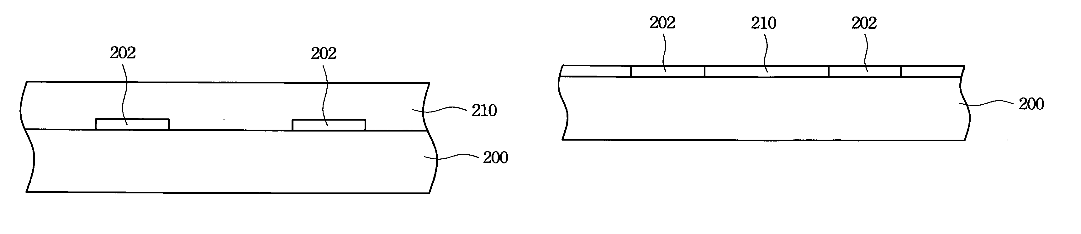
[0016]FIGS. 2A to 2F illustrate a series of cross views of a process for fabricating metal bumps in accordance with a preferred embodiment of the present invention. First, a substrate 200 with a plurality of pads 202 is provided (shown in FIG. 2A), wherein the substrate contains no solder mask formed thereon. In the present embodiment, the substrate 200 is but not limited as a printed circuit board (PCB), any substrate that has a circuit set thereon may be available. A first photoresist 210 is then formed on the substrate 200 to cover the pads 202. In the present embodiment, the first photoresist 210 may be an organic film or an inorganic film in a liquid phase that is formed by (but not limited to) a blade coating process, a roller coating process, spray coating process, a curtain coating process or a spin coating process. Otherwise, the first photoresist 210 may be an organic film or an inorganic film in a solid phase that is formed by a hot embossing process or a vacuum embossing...


PUM

PropertyMeasurementUnit
conductiveaaaaaaaaaa
thicknessaaaaaaaaaa
sizeaaaaaaaaaa

Abstract

A method for forming metal bumps is disclosed. Steps of the method include supplying a substrate containing a plurality of pads; forming a first photoresist layer on the substrate, herein the first photoresist layer covers the pads; performing a planarization step to remove a portion of the first photoresist layer so as to expose the pads; forming a conductive layer on the first photoresist layer and the pads; electroplating a metal layer on the conductive layer; forming a patterned second photoresist layer on the metal layer; a portion of the metal layer and the conductive layer which are not covered by the patterned second photoresist layer is removed by using the patterned second photoresist layer as a mask; removing the patterned second photoresist layer; and forming a solder mask on the substrate, wherein the solder mask has a plurality of openings to expose the metal layer located on the pads.

Description

RELATED APPLICATIONS[0001]The present application is based on, and claims priority from, Taiwan Application Serial Number 95109338, filed Mar. 17, 2006, the disclosure of which is hereby incorporated by reference herein in its entirety.FIELD OF THE INVENTION[0002]The present invention relates to a fine pitch package process, and more particularly to a method for fabricating metal bumps.BACKGROUND OF THE INVENTION[0003]FIGS. 1A to 1E illustrate a series of cross views of a conventional process for fabricating metal bumps. First, a substrate 100 with a plurality of pads 102 shown in FIG. 1A is provided. A patterned solder mask 110 is then formed on the substrate 100. The solder mask 110 is first formed to cover the substrate 100, and subsequently a patterning process, such as a photolithography process, is conducted on the solder mask 110 to form a plurality of first openings 112 exposing these pads 102. Next, a conductive layer 120 is formed over the patterned solder mask 110, wherei...

Claims


Application Information

Patent Timeline
Patent Type & Authority Applications(United States)
IPC IPC(8): H01L21/44
CPCH01L21/4853H01L24/11H01L2224/114H01L2224/116H01L2224/13082H01L2224/13111H01L2224/13113H01L2224/13116H01L2224/13139H01L2224/13147H01L2224/1357H01L2224/13611H01L2224/13613H01L2224/13616H01L2224/13618H01L2224/13624H01L2224/13639H01L2224/13644H01L2224/13647H01L2224/13655H01L2224/1366H01L2224/13664H01L2924/01011H01L2924/01013H01L2924/01029H01L2924/0103H01L2924/01046H01L2924/01047H01L2924/01075H01L2924/01078H01L2924/01079H01L2924/01082H05K3/064H05K3/28H05K3/4007H05K2201/0367H05K2201/09881H05K2203/054H05K2203/0542H05K2203/0574H01L2924/00013H01L2924/01019H01L2924/01033H01L2924/014H01L2224/11902H01L2924/00014H01L2224/13099
Inventor WANG, SHENG-MINGCHANG, SHUO-HSUNCHANG, KUO-HUAHUANG, CHI-CHIHCHEN, CHIH-CHENG
Owner ADVANCED SEMICON ENG INC
Why Eureka
Try Eureka