Method for manufacturing plastic packaging of MEMS devices and structure thereof

a technology of microelectromechanical systems and manufacturing methods, applied in the direction of fluid pressure measurement, fluid pressure measurement by electric/magnetic elements, instruments, etc., can solve the rare chance of short circuit between the bonding pad and the carrier, and achieve the effect of simplifying the process and increasing the yield ra

Inactive Publication Date: 2007-09-27
IND TECH RES INST
View PDF19 Cites 37 Cited by
  • Summary
  • Abstract
  • Description
  • Claims
  • Application Information

AI Technical Summary

Benefits of technology

[0010]According to the foregoing problems, the present invention provides a method for manufacturing a plastic packaging of MEMS devices and structure thereof, where gaskets are not necessary for forming a window above the sensitive area of the MEMS device, and multiple windows can be formed at the same time. Therefore, the process is simplified and the yield rate may be increased. Furthermore, a strong aci

Problems solved by technology

Therefore, chances that a short circuit between

Method used


Image

  • Method for manufacturing plastic packaging of MEMS devices and structure thereof
  • Method for manufacturing plastic packaging of MEMS devices and structure thereof
  • Method for manufacturing plastic packaging of MEMS devices and structure thereof

Examples


Embodiment Construction

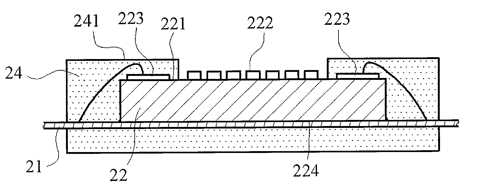
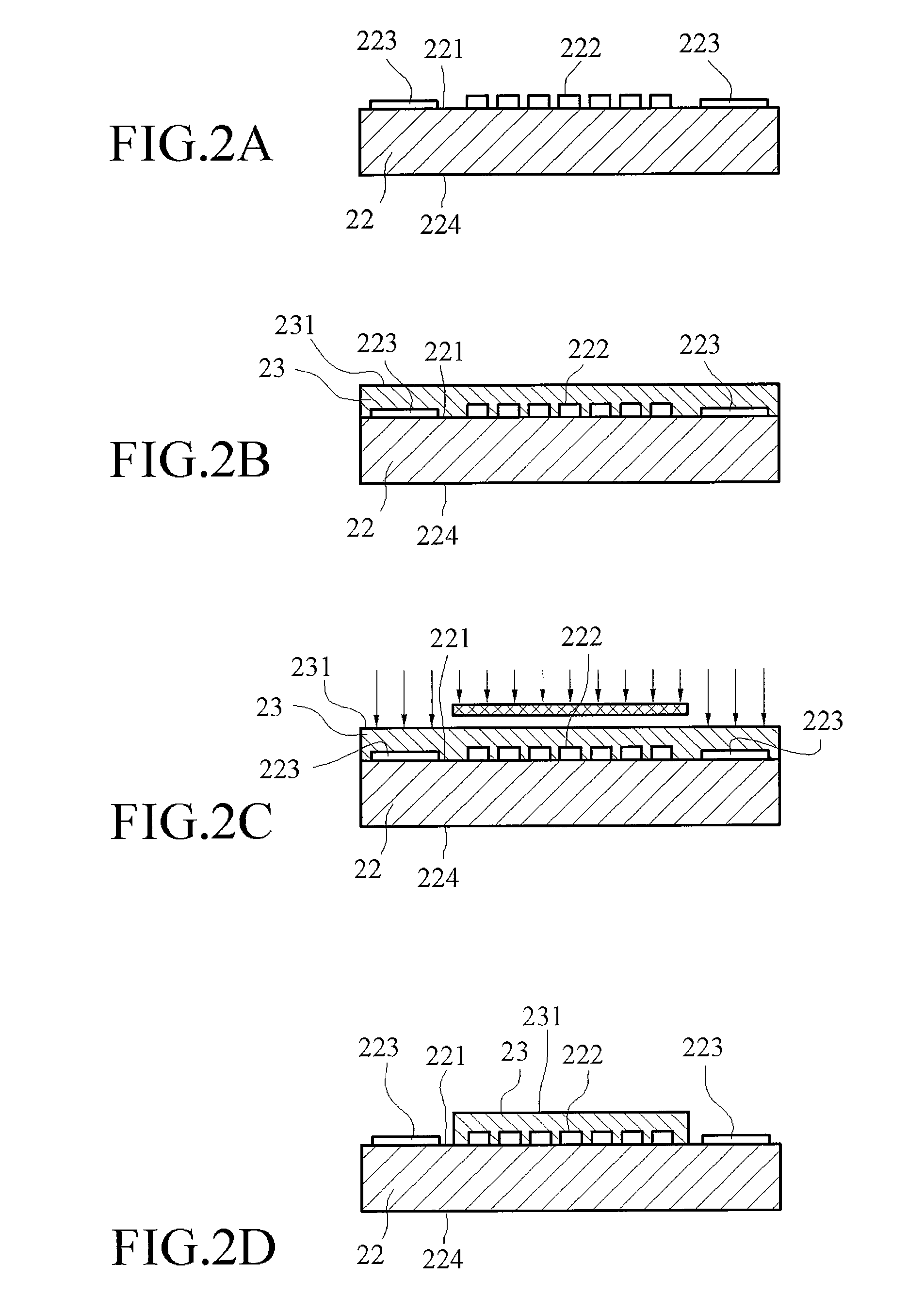
[0025]An embodiment of a method for manufacturing a plastic packaging of MEMS devices will be described with respect to FIGS. 2A to 2G First, a carrier 21, having a surface, is provided. The carrier 21 can be a PCB or a substrate, like a lead frame. Then at least one MEMS device 22 is provided, which has an active surface 221 and a back surface 224. There are a sensitive area 222 and bonding pads 223 on the active surface 221. Next, a photo-resist process is used to form a sacrifice layer 23 on the sensitive area 222 to protect the sensitive area against the follow-up encapsulating process. The sacrifice layer 23 can include a light-sensitive polymer material, such as SU-8 photoresist, and can be covered on the sensitive area 222 by spin coating, to form a uniform thickness of a photoresist layer (i.e. sacrifice layer23), or by a screen printing process with screen mask. The back surface 224 of the MEMS device 22 is bound to the surface of the carrier 21 by Au—Sn eutectic bonding, g...


PUM


Abstract

A plastic packaging of MEMS device and a method therefore are provided. The method includes the steps of: provide a carrier having a surface; provide at least one MEMS device having an active surface with a sensitive area and bonding pads thereon and a back surface; proceed a photoresist process to form a sacrificial layer on the sensitive area; bind and electrically connect the MEMS device to the surface of the carrier; form at least one molding compound, to which the upper surface of the sacrificial layer is exposed. Finally, decompose the sacrificial layer by a solvent to expose the MEMS device on the sensitive area, so as to let the sensitive area contact with ambient atmosphere.

Description

CROSS-REFERENCE TO RELATED APPLICATIONS[0001]This non-provisional application claims priority under 35 U.S.C. § 119(a) on Patent Application No(s). 095109928 filed in Taiwan, R.O.C. on Mar. 22, 2006, the entire contents of which are hereby incorporated by reference.BACKGROUND[0002]1. Field of Invention[0003]The invention relates to a method for manufacturing plastic packaging of microelectromechanical systems (MEMS) devices and structure thereof, and more particularly to a method of forming a space above the sensitive area of a MEMS device in a plastic packaging and structure thereof.[0004]2. Related Art[0005]Regarding to the microelectromechanical system (MEMS) industry, a MEMS device naturally has attractive features in microminiaturization and integration; however, the hardly reducible cost of MEMS device limits its application.[0006]On the other hand, a cell phone may become an information center which provides various information about daily life, such as environment temperatur...

Claims


Application Information

Patent Timeline
IPC IPC(8): H01L29/84H01L21/00
CPCB81C2203/0154B81C1/00896H01L2924/1815H01L2924/10155H01L2224/48091H01L2224/48247H01L2924/181H01L2924/00014H01L2924/00012H01L29/00H01L23/28
Inventor CHEN, JUNG-TAICHANG, WEN-YANGCHIOU, YII-TAYCHU, CHUN-HSUN
Owner IND TECH RES INST
Why Eureka
Try Eureka