Wiring structure, multilayer wiring board, and electronic device

Inactive Publication Date: 2007-09-27
KYOCERA CORP
View PDF1 Cites 20 Cited by
  • Summary
  • Abstract
  • Description
  • Claims
  • Application Information

AI Technical Summary

Benefits of technology

[0015]The present invention has originated in order to overcome the above problems in the related art. An object of the present invention is to provide a multilayer wiring board which facilitates characteristic impedance matching between an equilibrium transmission path and a non-equilibrium transmission path both of which are formed on the multilayer wiring board so as to obtain high wiring density and so as to be able to deal with high-speed operation of semiconductor elements.
[0016]According to an aspect of the present invention, capacitance between a differential signal line and a ground conductive layer decreases, thereby increasing a characteristic impedance of the differential signal line. As a result, each characteristic impedance of a general signal line and the differential signal line can be matched without adjusting a thickness of an insulation layer formed between the general signal line and the ground conductive layer so as to be widely different from a thickness of an insulation layer formed between the differential signal line and the ground conductive line, or without adjusting a wiring width of the differential signal line so as to be greater than a wiring width of the general signal line. Therefore, it becomes possible to increase wirin

Problems solved by technology

Therefore, wiring density cannot increase.
In practice, however, the thickness of the insulation layer needs to be partially changed, or the material of the insulation layer needs to be partially changed, which is not practic

Method used


Image

  • Wiring structure, multilayer wiring board, and electronic device
  • Wiring structure, multilayer wiring board, and electronic device
  • Wiring structure, multilayer wiring board, and electronic device

Examples


Embodiment Construction

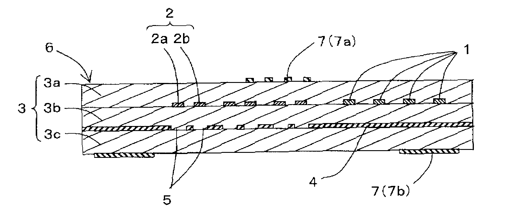
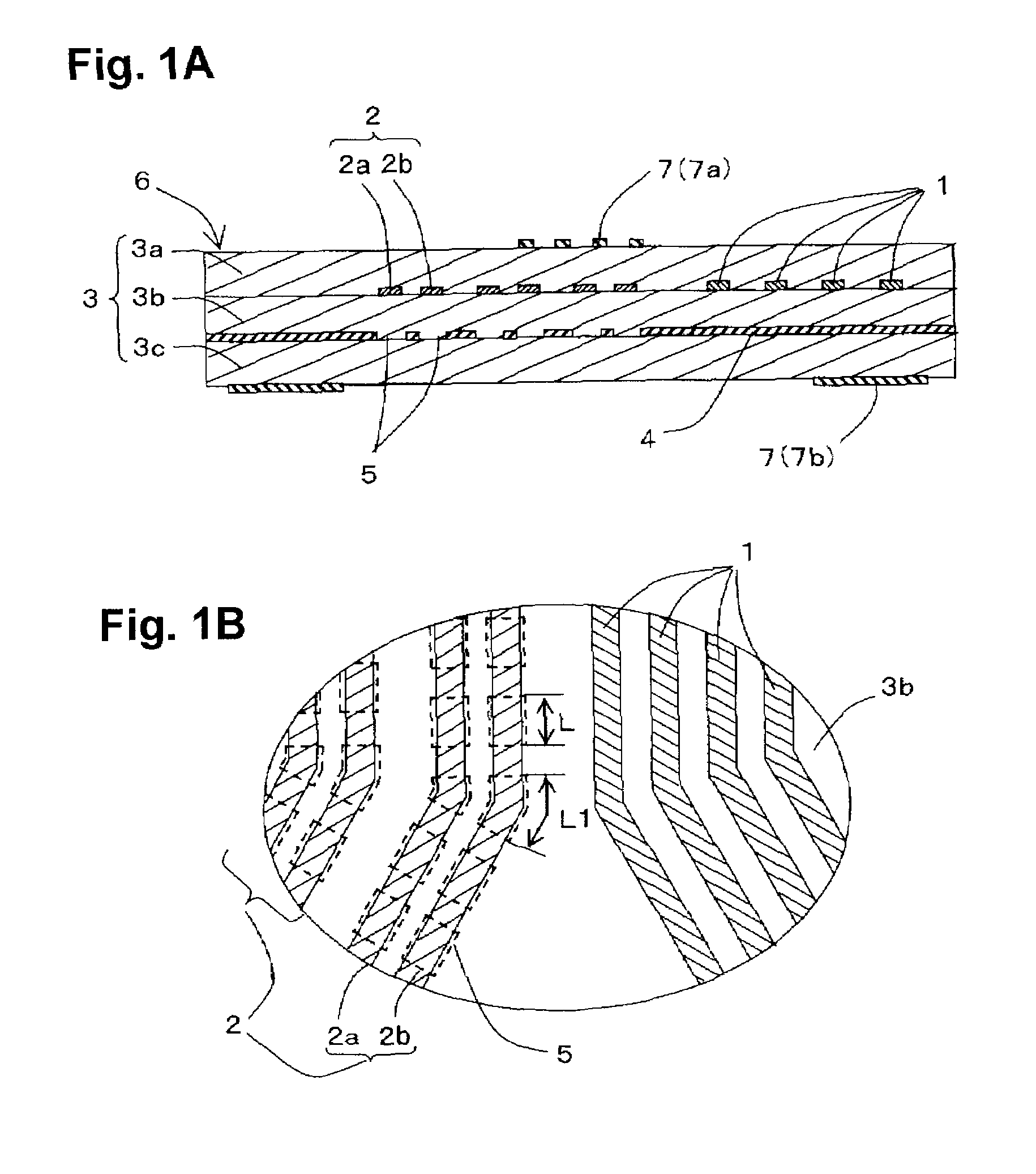
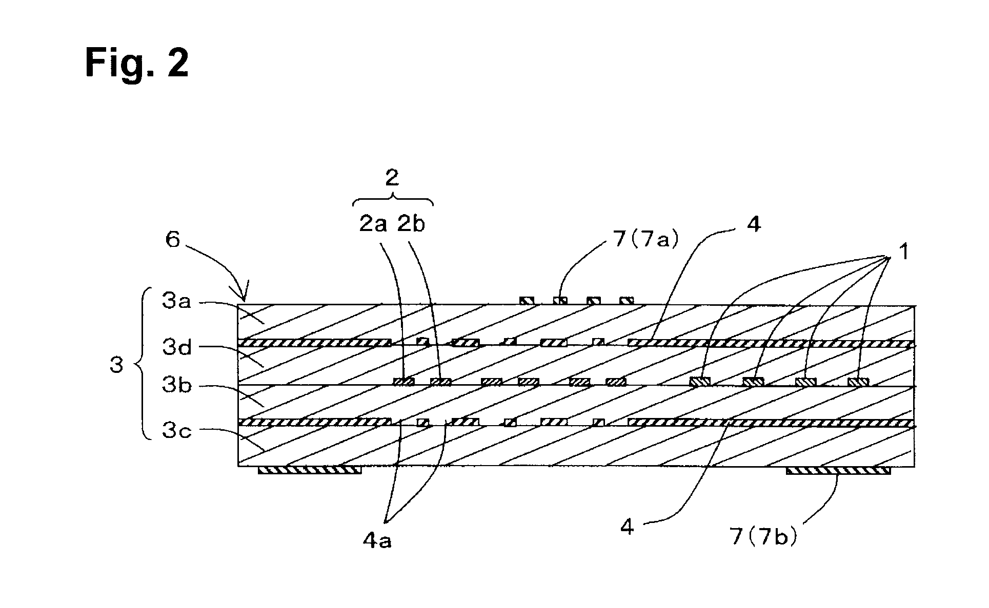
[0026]Hereinafter, a multilayer wiring board of the present invention will be described in detail. FIG. 1 is a view illustrating a multilayer wiring board according to an embodiment of the present invention, in which FIG. 1A is a cross-sectional view of the multilayer wiring board of the present invention, and FIG. 1B is an enlarged view of a substantial part of FIG. 1A, viewed from the top. Referring to the figures, provided are a general signal line 1, a differential signal line 2, a first signal line path 2a constituting the differential signal line 2, a second signal line path 2b constituting the differential signal line 2, an insulation layer 3, a ground conductive layer 4 acting as a reference potential layer, a non-formed portion (hereinafter, referred to as an opening portion) 5 in the ground conductive layer 4, a multilayer wiring board 6, and a surface wiring line 7.

[0027]In the present invention, the reference potential layer includes a so-called ground conductive layer a...


PUM


Abstract

A wiring structure includes a general signal line, a differential signal line having a pair of signal wiring lines and a reference potential layer. The signal wiring lines respectively transmit differential signals of which waveforms are inverted from each other. The reference potential layer is arranged to have a distance from the general signal line and the differential signal line, and has a non-formed portion in a region to be electromagnetically coupled to the differential signal line.

Description

CROSS-REFERENCE TO RELATED APPLICATIONS[0001]The present application claims priority under 35 U.S.C. §119 to Japanese Patent Application No. 2006-83154, filed Mar. 24, 2006, entitled “WIRING STRUCTURE, MULTILAYER WIRING BOARD, AND ELECTRONIC DEVICE.” The contents of this application are incorporated herein by reference in their entirety.BACKGROUND OF THE INVENTION[0002]1. Field of the Invention[0003]The present invention relates to an wiring structure having a differential signal line suitable for connecting such electronic elements as rapidly-operating semiconductor elements, optical semiconductor elements, etc, a multilayer wiring board, and an electronic device using the same, and more particularly, to an wiring structure having a differential signal line and a general signal line, a multilayer wiring board, and an electronic device.[0004]2. Description of the Related Art[0005]Conventionally, such electronic elements as representative semiconductor elements, e.g. for a microproce...

Claims


Application Information

Patent Timeline
IPC IPC(8): H01L23/02
CPCH01L23/49822H01L23/50H01L2924/0002H01L23/66H01L2223/6627H01L2924/09701H01L2924/1903H01L2924/3011H01P3/08H05K1/0224H05K1/0245H05K1/0253H05K1/0298H05K2201/09236H05K2201/093H05K2201/0969H01L2223/6638H01L2924/00
Inventor KABUMOTO, MASANAO
Owner KYOCERA CORP
Why Eureka
Try Eureka