Method of Driving Plasma Display Panel

a plasma display and plasma technology, applied in static indicating devices, instruments, gas-filled discharge tubes, etc., can solve the problems of rapid decrease, and difficult to conduct the address discharg

Inactive Publication Date: 2007-09-27
PANASONIC CORP
View PDF1 Cites 16 Cited by
  • Summary
  • Abstract
  • Description
  • Claims
  • Application Information

AI Technical Summary

Problems solved by technology

However, there are several factors delaying the discharges, e.g. a high voltage cannot be used to an address pulse voltage due to constraints of the circuit structure, or the phosphor layer formed on the data electrodes make it difficult to conduct the address discharges.
The priming generated by the discharges, however, decreases rapidly with the passage of time, so that the priming generated by the initial discharge becomes in short supply for the address discharge to be conducted long after the initial discharge.
As a result, the discharge delays longer, which makes the address operation unstable and lowers the video quality, or an address time is set longer in order to make the address operation stable, so that the address operation resultantly takes too much time.
This panel, however, tends to invite interference between discharge cells adjacent to each other.
Particularly in the addressing period, the discharge of the discharge cells adjacent to each other produces some priming which sometimes causes an address error or an address defective.

Method used


Image

  • Method of Driving Plasma Display Panel
  • Method of Driving Plasma Display Panel
  • Method of Driving Plasma Display Panel

Examples


Embodiment Construction

Exemplary Embodiment

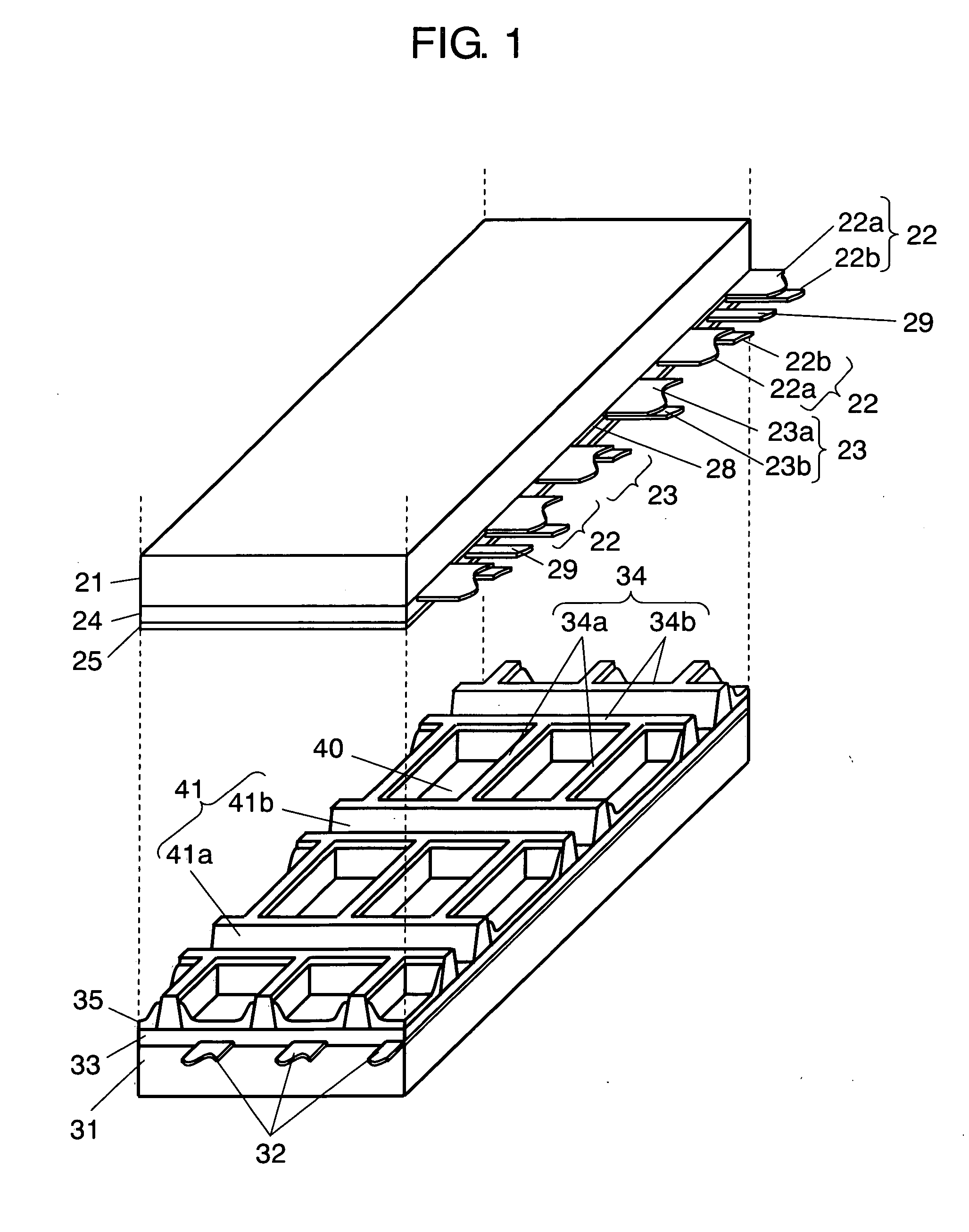
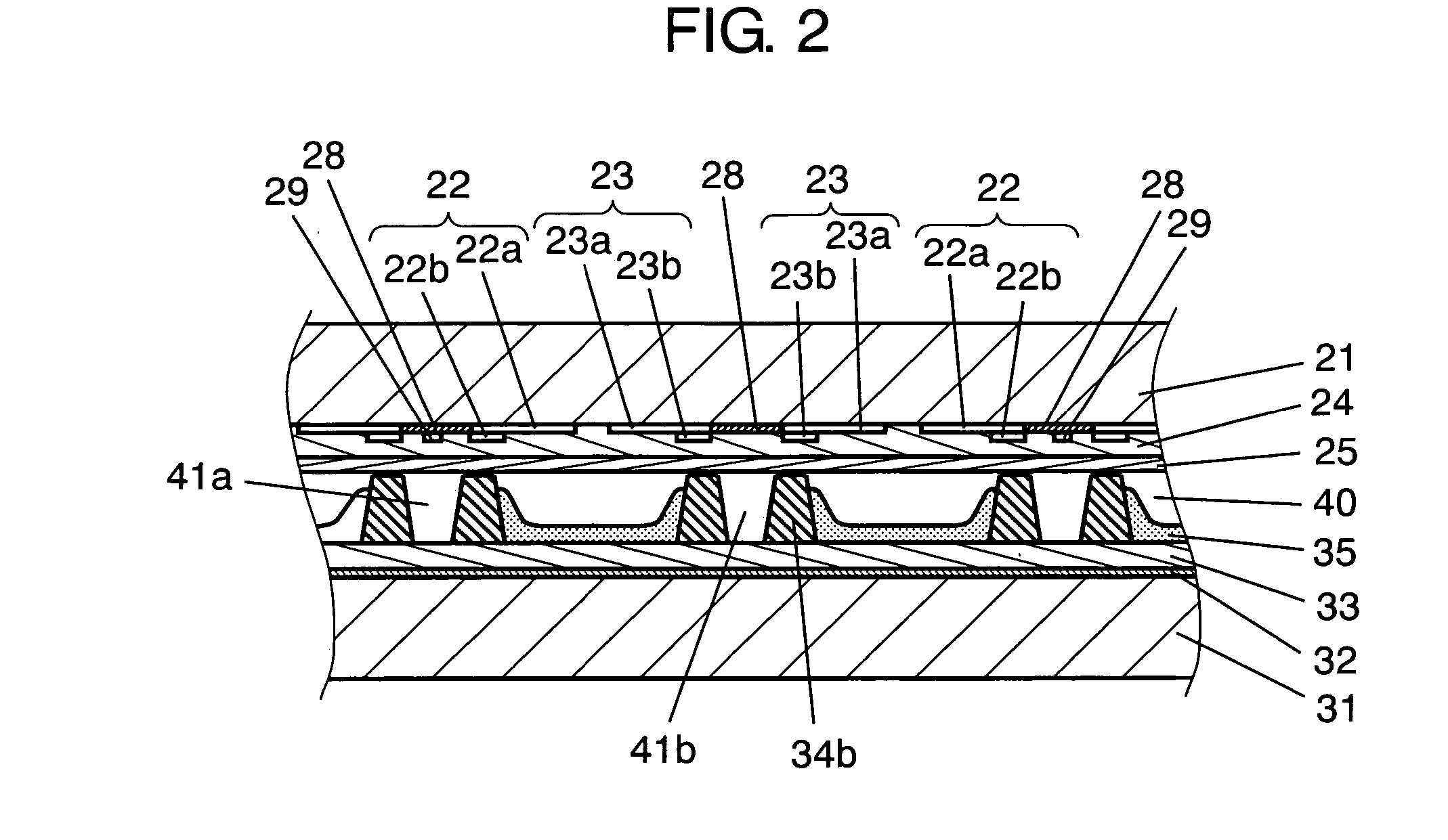
[0046]FIG. 1 shows a perspective exploded view illustrating a structure of a panel in accordance with this embodiment of the present invention. FIG. 2 shows a sectional view illustrating the same panel. A first substrate, i.e. front substrate 21 made of glass, confronts a second substrate, i.e. rear substrate 31, with a discharge space in between. The discharge space is filled with mixed gas of neon and xenon for radiating ultraviolet ray by discharging.

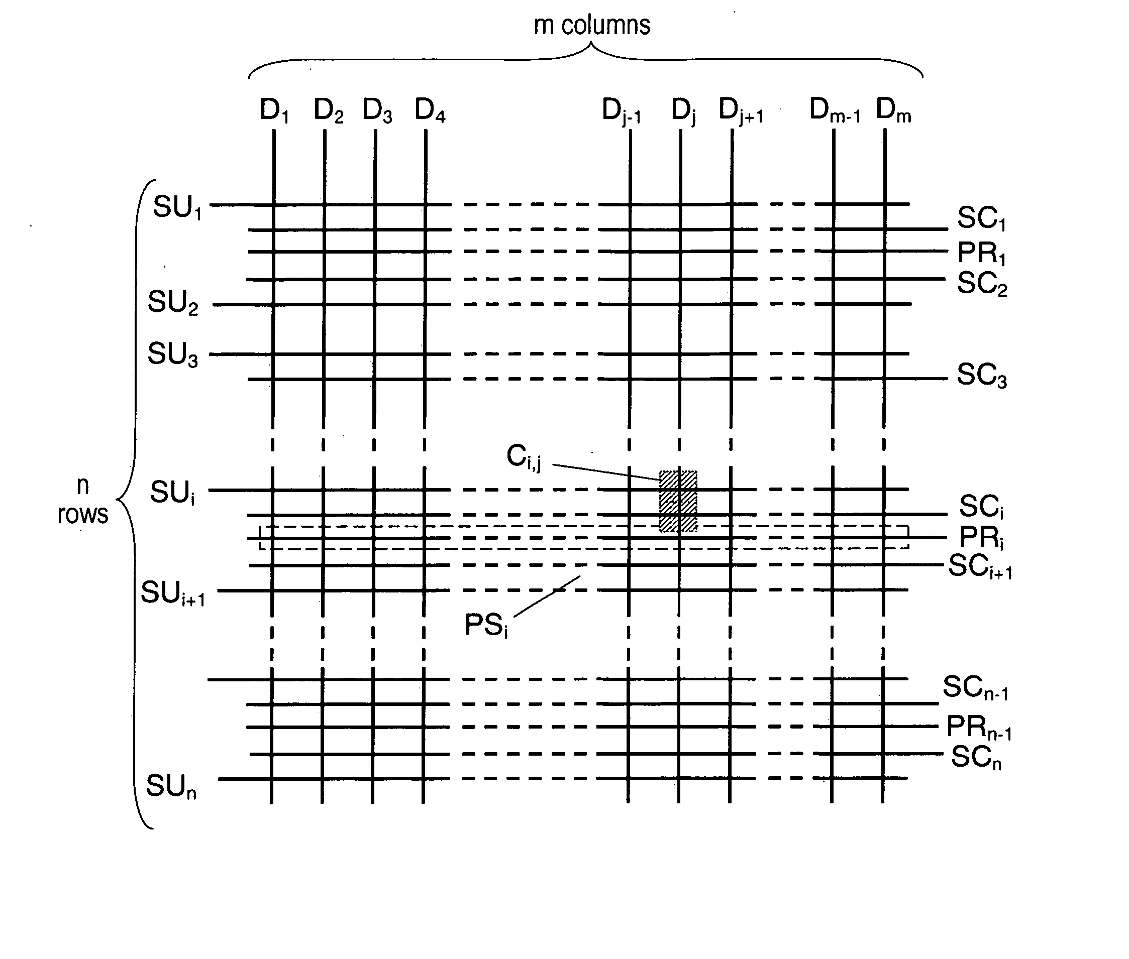
[0047] A plurality of display electrode pairs, each one of which pair is formed of scan electrode 22 and sustain electrode 23, are formed on front substrate 21 such that scan electrodes 22 and sustain electrodes 23 are placed in parallel with each other. For instance, a display electrode pair, formed of scan electrode 22 first and sustain electrode 23 second in this order, is adjacent to another display electrode pair formed of sustain electrode 23 first and scan electrode 22 second in this order. There are spac...


PUM


Abstract

A method of driving a plasma display panel having display electrode pairs each one of which pairs is formed of a scan electrode and a sustain electrode. A priming electrode is placed in every other spaces between the display electrode pairs and in parallel with the display electrode pairs. An addressing period includes an odd-line addressing period in which an address operation is conducted to primary discharge cells having odd-number scan electrodes, an even-line addressing period in which an address operation is conducted to primary discharge cells having even-number scan electrodes. During the respective addressing periods, scan pulse voltage Va is applied to odd-number scan electrodes or even-number scan electrodes while priming pulse voltage Vp is applied, prior to the application of the scan pulse voltage, to a priming electrode adjacent to the scan electrode to which scan pulse voltage Va is to be applied, in order to generate a priming discharge between the priming electrodes and the data electrodes.

Description

TECHNICAL FIELD [0001] The present invention relates to a method of driving plasma display panels to be used in wall-mounted television receivers or large-size monitors. BACKGROUND ART [0002] A plasma display panel (hereinafter simply referred to as “panel”) is a display device excellent in visibility and features a large size, thin and light weight screen. [0003] An AC surface discharge panel, one of typical panels, comprises numbers of discharging cells formed between a front plate and a back plate confronting each other. The front plate comprises display electrode pairs each one of which pair is formed of a scan electrode and a sustain electrode, and the display electrode pairs are formed in parallel to each other on a front glass substrate. A dielectric layer and a protective layer are formed such that those two layers cover the display electrodes. The back plate comprises a plurality of data electrodes formed on a back glass substrate in parallel to each other, a dielectric lay...

Claims


Application Information

Patent Timeline
Patent Type & Authority Applications(United States)
IPC IPC(8): G09G3/28G09G3/20G09G3/292G09G3/288G09G3/291G09G3/293G09G3/298H01J11/14H01J11/22H01J11/24H01J11/28H01J11/34H01J11/36
CPCG09G3/2007G09G3/2927G09G2310/0218G09G3/294G09G3/2986G09G3/293G09G3/292H01J11/28
Inventor TACHIBANA, HIROYUKIKOSUGI, NAOKIWAKABAYASHI, TOSHIKAZUOKUMURA, SHIGEYUKI
Owner PANASONIC CORP
Why Eureka
Try Eureka