On-chip ESD protection circuit for compound semiconductor heterojunction bipolar transitor RF circuits

a protection circuit and heterojunction technology, applied in the direction of emergency protective circuit arrangements, emergency protective arrangements for limiting excess voltage/current, emergency protective arrangements, etc., can solve the problems of circuits affecting power gain, linearity, bandwidth, circuits can affect the size of diodes in the string b>10/b>, and achieve the effect of minimizing leakage current and improving linearity

Inactive Publication Date: 2007-09-27
RGT UNIV OF CALIFORNIA
View PDF4 Cites 21 Cited by
  • Summary
  • Abstract
  • Description
  • Claims
  • Application Information

AI Technical Summary

Benefits of technology

[0019] Again the triggering of the transistor switch preferably comprises triggering a Darlington pair. The triggering of the Darlington pair comprises coupling the first type of ESD event through the diode string to the gate of the Darlington pair while also coupling the first type of ESD event through the diode string to a series diode and resistor to ground to prevent the ESD protection circuit from turning on during low to moderate RF power operation, therefore minimizing leaking current and improving linearity.

Problems solved by technology

The thin epitaxy active layers are prone to damages from an ESD event.
The capacitance loading from the ESD protection circuit can affect power gain, linearity, and bandwidth.
The major drawback of the ESD protection circuit of FIG. 2 is that the size of the diodes in the string 10 needs to be big in order to reduce the parasitic resistance.

Method used


Image

  • On-chip ESD protection circuit for compound semiconductor heterojunction bipolar transitor RF circuits
  • On-chip ESD protection circuit for compound semiconductor heterojunction bipolar transitor RF circuits
  • On-chip ESD protection circuit for compound semiconductor heterojunction bipolar transitor RF circuits

Examples


Embodiment Construction

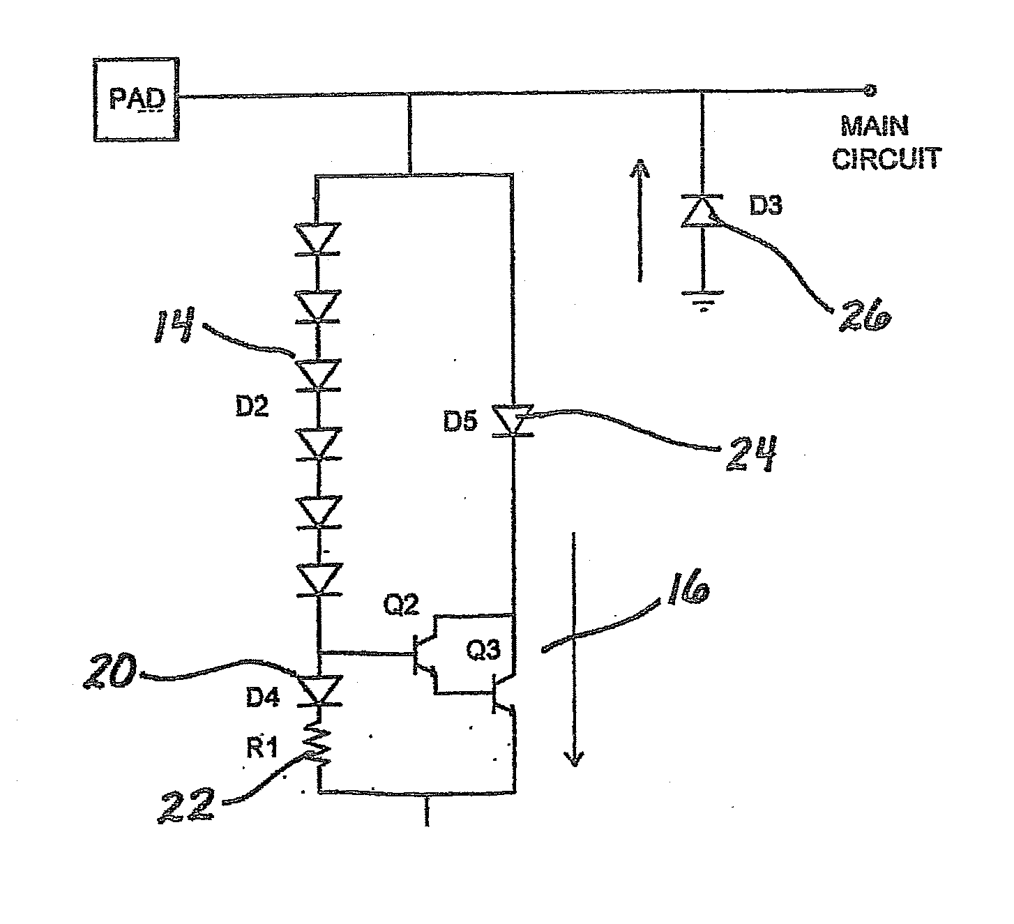
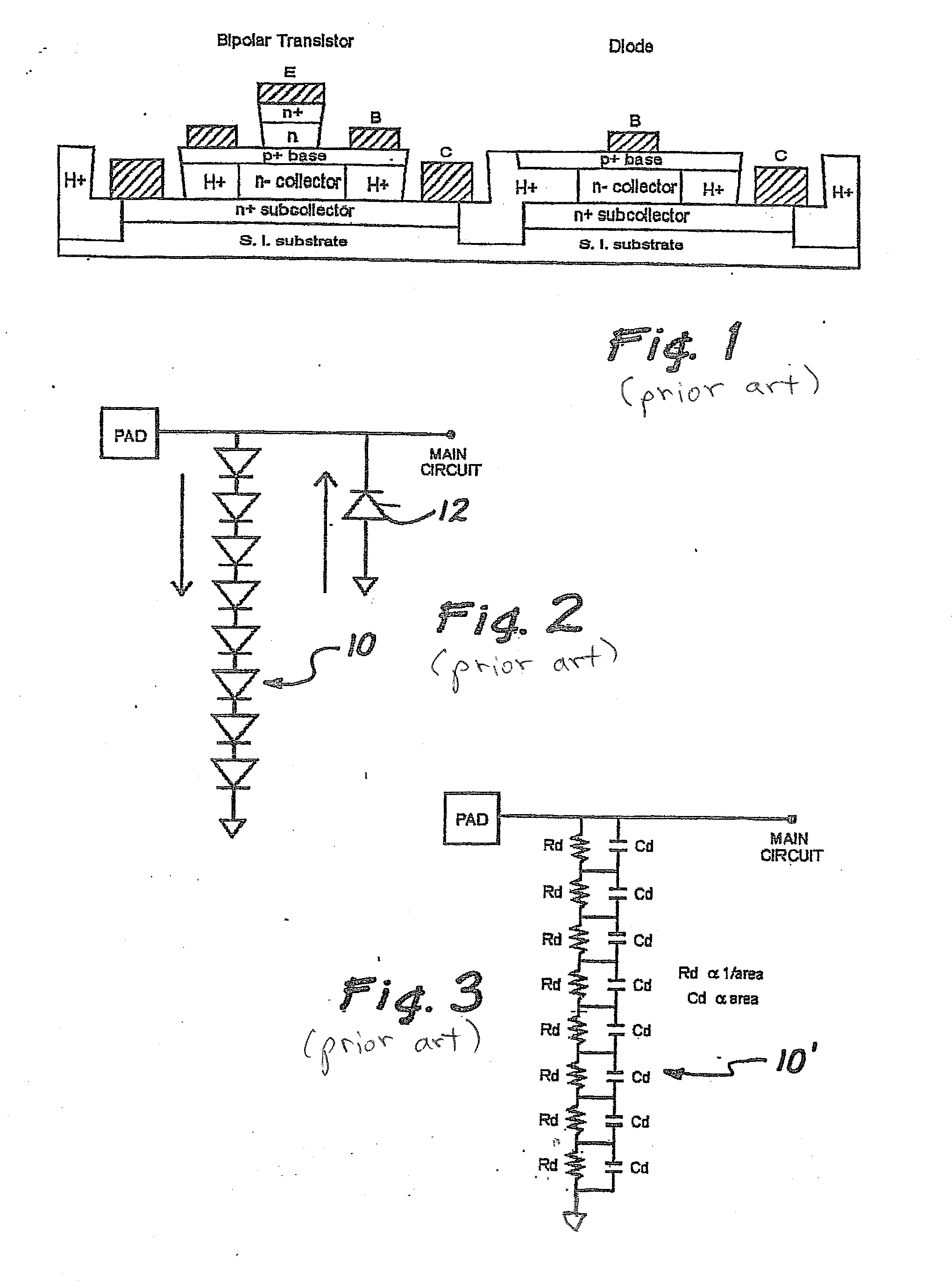
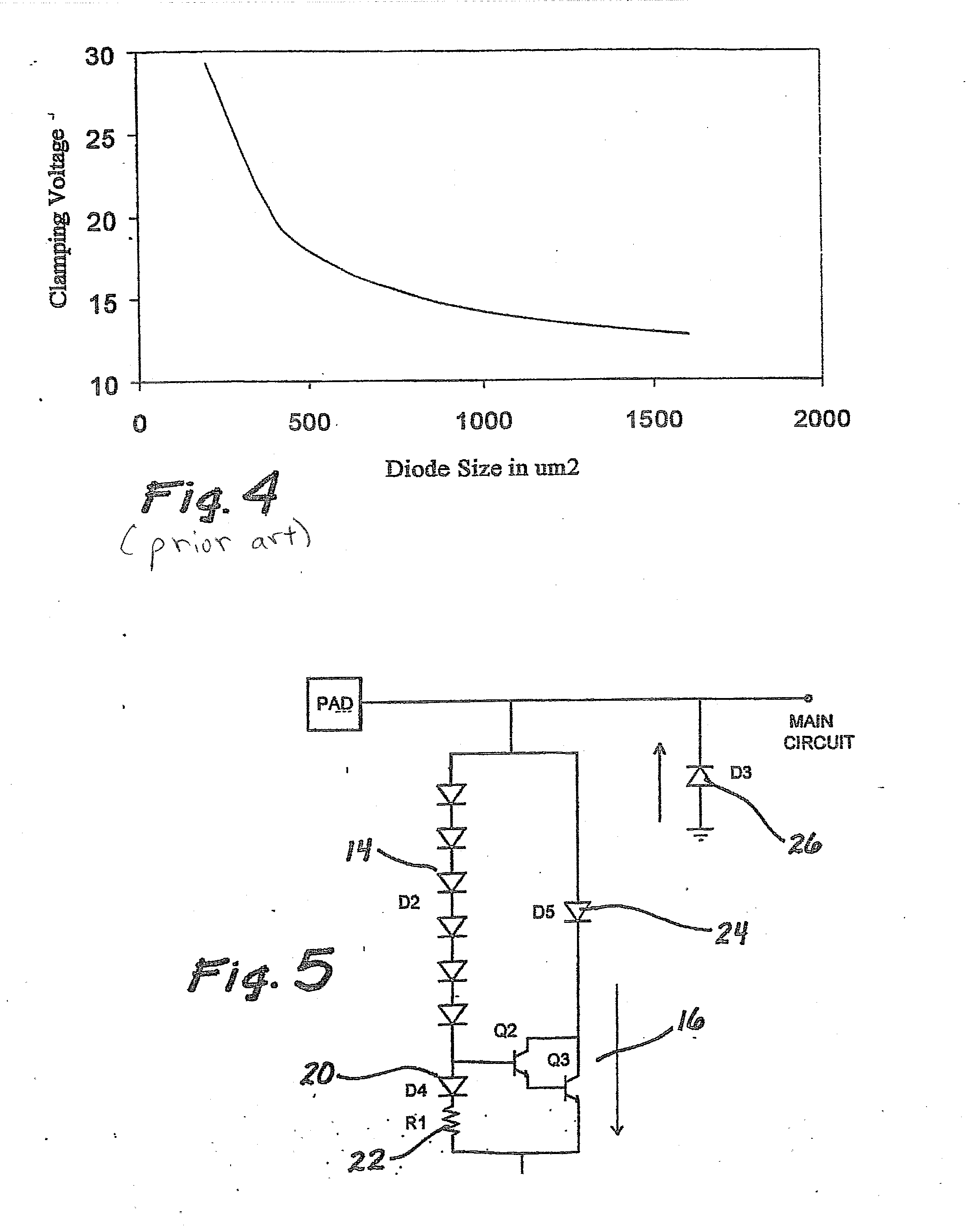
[0046] As illustrated in one of the compound semiconductor heterojunction bipolar transistor (HBT) technology, a low loading capacitance on-chip electrostatic discharge (ESD) protection circuit for GaAs power amplifiers is disclosed, which does not degrade the circuit RF performance. The similar method can be applied to other technologies included InP, SiGe, etc., Its principle of operation and simulation results regarding capacitance loading, leakage current, degradation to RF performance are disclosed. The design, loading effect over frequency, robustness over process and temperature variation and application to an RF power amplifier is presented in detail. The ESD circuit couples an input to ground during ESD surges through a diode string coupled to the input, and a transistor switch or Darlington pair 16 having its gate coupled to and triggered by the diode string. The Darlington pair 16 couples the input to ground when triggered through a low impedance path in parallel to the d...


PUM


Abstract

A low loading capacitance on-chip electrostatic discharge (ESD) protection circuit for compound semiconductor power amplifiers is disclosed, which does not degrade the circuit RF performance. Its principle of operation and simulation results regarding capacitance loading, leakage current, degradation to RF performance are disclosed. The design, loading effect over frequency, robustness over process and temperature variation and application to an RF power amplifier is presented in detail. The ESD circuit couples an input to ground during ESD surges through a diode string coupled to the input, and a transistor switch or Darlington pair having its gate coupled to and triggered by the diode string. The Darlington pair couples the input to ground when triggered through a low impedance path in parallel to the diode string. A reverse diode also couples ground to the input on reverse surges.

Description

RELATED APPLICATIONS [0001] The application is a continuation of application Ser. No. 10 / 501,651, filed on Jan. 10, 2005, which in turn was related to U.S. Provisional Patent Application Ser. No. 60 / 349,899, filed on Jan. 18, 2002, which is incorporated herein by reference and to which priority is claimed pursuant to 35 USC 119.BACKGROUND OF THE INVENTION [0002] 1. Field of the Invention [0003] The invention relates to the field of electrostatic discharge (ESD) protection circuits and in particular to a low loading capacitance on-chip electrostatic discharge (ESD) protection circuit for compound semiconductor (such as GaAs, InP, SiGe etc) heterojunction bipolar transistor RF circuits. [0004] 2. Description of the Prior Art [0005] Compound semiconductor heterojunction bipolar transistors (HBT) are attractive for RF integrated circuits (RFIC). For example, due to the high electron mobility, high current gain, low base resistance, and low loss semi-insulated substrate, a GaAs heterojun...

Claims


Application Information

Patent Timeline
Patent Type & Authority Applications(United States)
IPC IPC(8): H02H9/00H01L27/02
CPCH01L27/0259H01L27/0255
Inventor MA, YIN TATLI, GUANN PYNG
Owner RGT UNIV OF CALIFORNIA
Why Eureka
Try Eureka