Semiconductor device and manufacturing method thereof

a technology of semiconductor and manufacturing method, applied in the direction of semiconductor/solid-state device manufacturing, semiconductor devices, electrical devices, etc., can solve the problems of unstable ohmic properties and formed schottky barrier, and achieve the effect of reliable ohmic electrodes

Active Publication Date: 2007-10-04
SUMITOMO ELECTRIC DEVICE INNOVATIONS
View PDF15 Cites 72 Cited by
  • Summary
  • Abstract
  • Description
  • Claims
  • Application Information

AI Technical Summary

Benefits of technology

[0016]Due to this, it has been made possible to suppress the electrode surface from becoming coarse [refer to FIG. 8(A) and FIG. 8(B)]. Further, it has been made possible to suppress the movement (electromigration) of the Al atom during operation at high temperatures.
[0017]Thus, by using the Ta / Al stacked structure for the source electrode 6 and the drain electrode 7 as an ohmic electrode, it has been made possible to realize sufficient reliability in a high temperature environment.
[0020]Aspect of the present invention can provide a semiconductor device and manufacturing method thereof that have been made capable of improving reliability of an ohmic electrode in a high humidity environment while securing sufficient reliability of an ohmic electrode in a high temperature environment.
[0023]Therefore, according to the semiconductor device and its manufacturing method of the above aspects of the present invention, there is an advantage that reliability of an ohmic electrode in a high humidity environment can be improved while securing sufficient reliability of an ohmic electrode in a high temperature environment.

Problems solved by technology

By the way, as described above, in a GaNFET that uses the Ti / Al electrode or the Ti / Al / Ni / Au electrode as an ohmic electrode, the work function of Ti is 4.3 eV, therefore, there is a problem that a Schottky barrier is formed in between with an n-type III-V group nitride compound semiconductor.
These constitute factors that make the ohmic properties unstable at the time of device process or during operation at high temperatures.

Method used


Image

  • Semiconductor device and manufacturing method thereof
  • Semiconductor device and manufacturing method thereof
  • Semiconductor device and manufacturing method thereof

Examples


Embodiment Construction

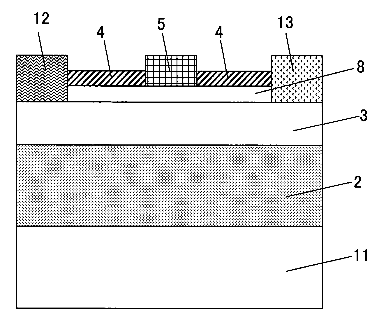
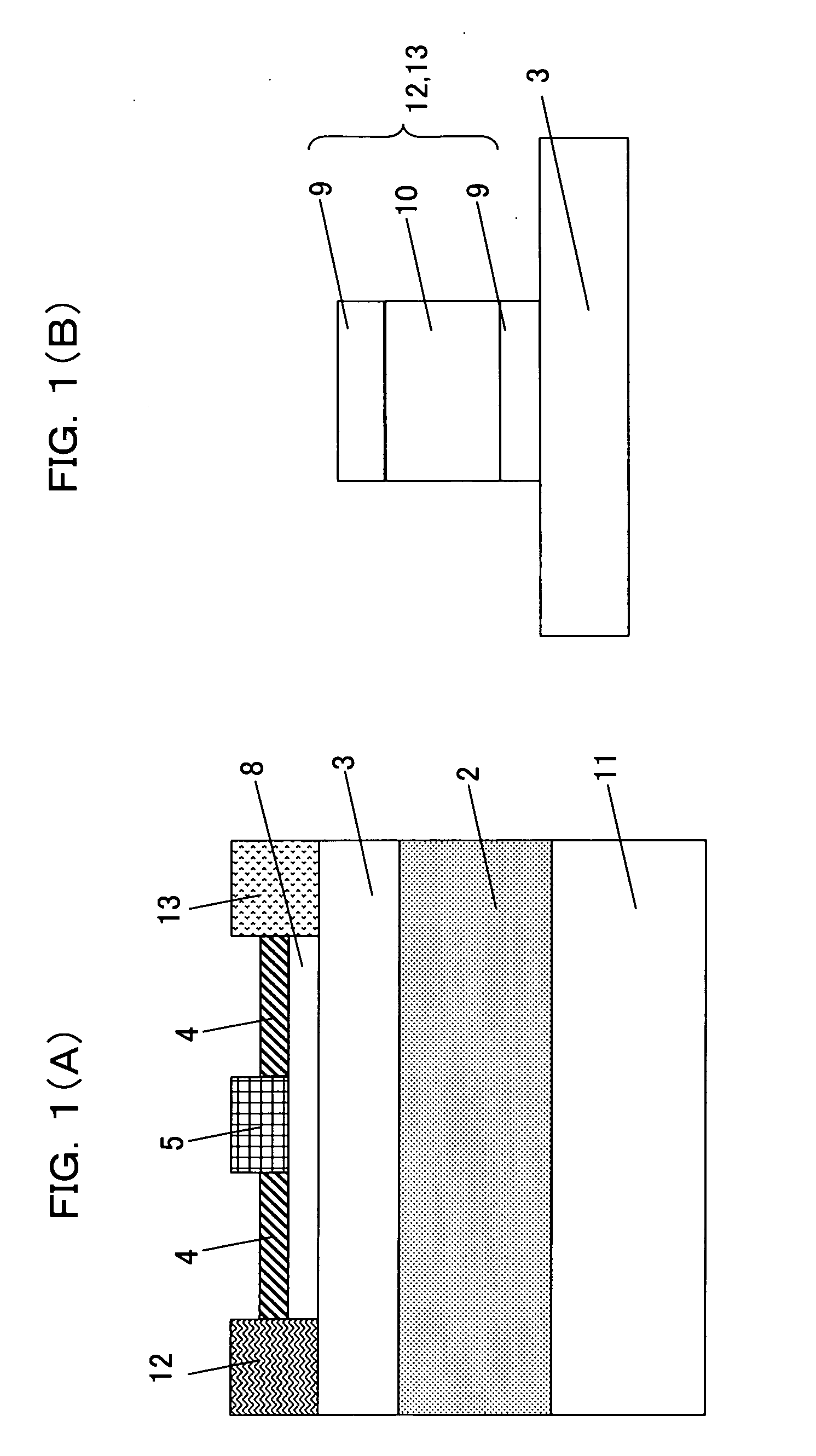
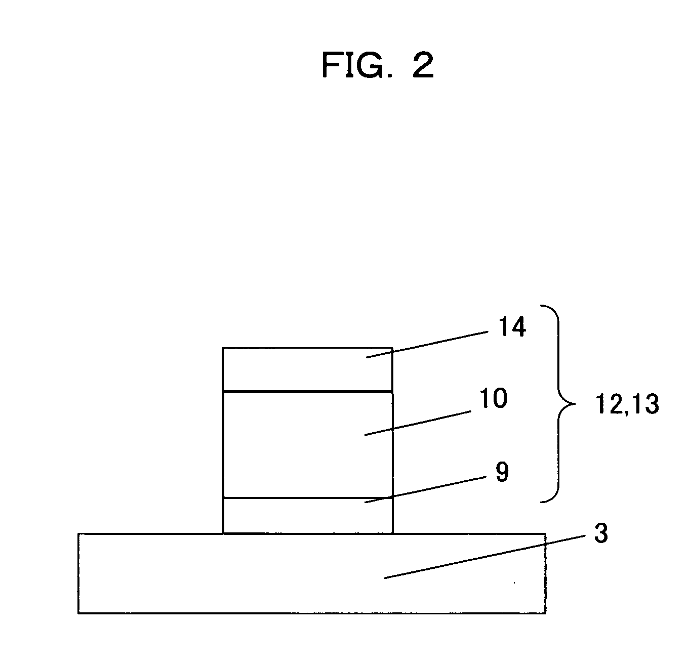
[0038]A semiconductor device and manufacturing method thereof according to an embodiment of the present invention are described below with reference to FIG. 1(A), FIG. 1(B), FIG. 2, and FIG. 3(A) to FIG. 3(J).

[0039]The semiconductor device (compound semiconductor device) according to the present embodiment is, for example, a gallium nitride based field effect transistor (GaNFET; here, HEMT; High Electron Mobility Transistor), and has, for example as shown in FIG. 1(A) and FIG. 1(B), a structure in which an intentionally undoped GaN electron transit layer 2 (i-GaN layer) 2, an electron supply layer 3 made of an n-type AlxGa1-xN (0≦x≦1) layer (n-AlGaN layer), and an n-type GaN layer (n-GaN layer) 8 are stacked in order on an SiC (silicon carbide) substrate 11. By the way, a spacer layer [for example, an intentionally undoped AlxGa1-xN (0≦x≦1) layer (i-AlGaN layer)] may be provided between the electron transit layer 2 and the electron supply layer 3.

[0040]On the n-type GaN layer (n-GaN...


PUM

PropertyMeasurementUnit
resistivityaaaaaaaaaa
temperaturesaaaaaaaaaa

Abstract

A semiconductor device is configured so as to comprise a substrate, an n-type semiconductor layer or an undoped semiconductor layer on the substrate, and an ohmic electrode on the n-type semiconductor layer or the undoped semiconductor layer, and the ohmic electrode is configured so as to comprise a tantalum layer formed on the n-type semiconductor layer or the undoped semiconductor layer, an aluminum layer formed on the tantalum layer, and a metal layer formed on the aluminum layer and made of any one material of tantalum, nickel, palladium, and molybdenum.

Description

CROSS REFERENCE TO RELATED APPLICATIONS[0001]This application is based on and hereby claims priority to Japanese Application No. 2006-094576 filed on Mar. 30, 2006 in Japan, the contents of which are hereby incorporated by reference.BACKGROUND OF THE INVENTION[0002](1) Field of the Invention[0003]The present invention relates to a semiconductor device and manufacturing method thereof suitable for use in, for example, a gallium nitride based field effect transistor (GaNFET).[0004](2) Description of Related Art[0005]Recently, development of a GaNFET (gallium nitride field effect transistor) is actively in progress, which makes use of an AlGaN / GaN hetero junction and the electron transit layer of which is GaN (gallium nitride).[0006]Because of being a material having a wide band gap, a high breakdown electric field strength, and a large saturation electron speed, GaN is highly promising as a material of a high power output device for which a high voltage operation is required.[0007]At ...

Claims


Application Information

Patent Timeline
Patent Type & Authority Applications(United States)
IPC IPC(8): H01L31/00H01L29/739
CPCH01L29/2003H01L29/41725H01L29/452H01L21/28575H01L29/7787
Inventor KANAMURA, MASAHITONISHI, MASAHIRO
Owner SUMITOMO ELECTRIC DEVICE INNOVATIONS
Why Eureka
Try Eureka