Liquid crystal display apparatus

a liquid crystal display and control structure technology, applied in non-linear optics, instruments, optics, etc., can solve the problems of constant generation of light leakage current, difficulty in improving the transmittance of back light without reducing the use efficiency of back light sources,

Inactive Publication Date: 2007-10-04
HITACHI DISPLAYS
View PDF8 Cites 35 Cited by
  • Summary
  • Abstract
  • Description
  • Claims
  • Application Information

AI Technical Summary

Benefits of technology

[0013]It is an object of the present invention to provide a high-luminance, high-definition liquid crystal display apparatus by efficiently passing light of a back light through a liquid crystal display panel.
[0014]The present invention achieves the object described above by including a phase shift structure in a transparent substrate forming a liquid crystal display panel. In the present invention, the phase shift structure described above composed of an existence pattern of a uniform film thickness is formed with a transparent substance having a refractive index different from that at the periphery thereof by only Δn, and the phase of light passing through a layer of the transparent substance is obtained by shifting the phase of light at the periphery thereof by approximately a half wavelength with respect to a wavelength of 550 nm. At the end of this layer of the transparent substance, a region canceling the light extends in the light traveling direction, and regions intensifying the light extend, on both sides thereof, from the end part at certain angles. Using this characteristic permits formation of a microlens with the phase shift structure.
[0015]For example, results of numerical analysis on a light condensing state for a width of 4 micrometer (μm) show that the phase shift structure optimally designed for a wavelength of 550 nm has lens effect over the entire wavelengths from 400 nm to 700 nm. This structure is called “phase shift element”. Forming, on the same transparent substrate where a thin-film transistor is formed (hereinafter also called a glass substrate), this phase shift element in accordance with an aperture part pattern inside a pixel permits efficient light condensation on the aperture part. Moreover; a photolitho process in a TFT formation process can be used for the formation of this phase shift element, thus making it easy to make position adjustment. Further, installation at a close distance in the depth direction from the aperture part through which light is transmitted is possible, so that the permitted limit for the width of distribution of incident light angles for condensing incident light on the aperture part increases, which permits condensation of in-plane light intensity distribution on the aperture part even by use of a back light source having wide incidence angle distribution.
[0017]According to the present invention, reducing light entering a TFT part by a phase shift element reduces the amount of light leak in a top gate type TFT and permits a reduction in the area of an auxiliary capacitance part, which in turn permits an improvement in the area of an aperture part.
[0018]According to the present invention, the light transmittance of an entire liquid crystal display panel becomes larger than a product of the aperture ratio of the entire liquid crystal display panel and the transmittance of the aperture part, thereby permitting providing a high-luminance, high-definition liquid crystal display apparatus with low power consumption.
[0024]According to another aspect of the present invention, in a liquid crystal display panel using a normal back light source, arranging light distributed to a non-aperture part at an aperture part again improves the light energy efficiency. As a result, the effective transmittance of the liquid crystal display panel improves. Moreover, for a liquid crystal display panel using a top gate type TFT, the area of an auxiliary capacitance part can be reduced, so that the transmittance improves as a result of an increase in the area of the aperture part.

Problems solved by technology

That is, light of a back light is wasted by the light shielding regions.
With past technology, a liquid crystal display panel, which is required to have a large view angle, has difficulty in improving its transmittance without reducing the use efficiency of a back light source.
In this case, the liquid crystal display panel is structured such that light of a back light directly enters a TFT channel region, thus resulting in drawbacks that light leak current is constantly generated at the TFT when the back light is turned on and that leak current is large even when the TFT is off.
This auxiliary capacitance part requires a very large area; therefore, the area of an aperture part becomes small by being compressed by the area of this auxiliary capacitance part, thus resulting in a problem of decreased transmittance.

Method used


Image

  • Liquid crystal display apparatus
  • Liquid crystal display apparatus
  • Liquid crystal display apparatus

Examples


first embodiment

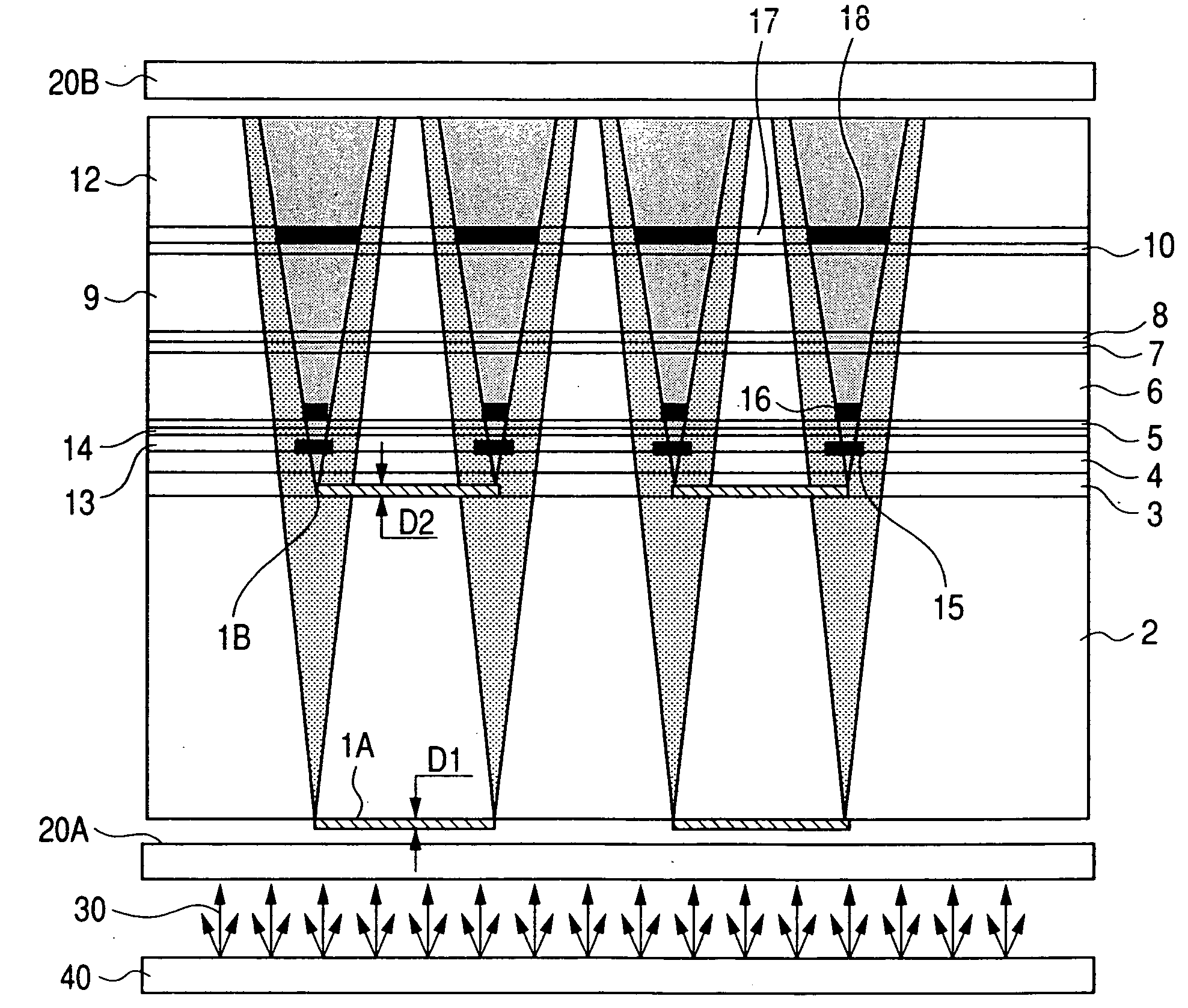
[0044]FIG. 1 is a schematic sectional view describing a first embodiment of a liquid crystal display apparatus according to the present invention. This liquid crystal display apparatus is a so-called IPS system (transverse electric field system). In this figure, an arrangement of wires, an electrode, a thin-film transistor, a pixel electrode, an opposite electrode, an insulating layer, and the like is shown in a conceptual diagram. Therefore, the arrangement and structure of these wires, electrode, thin-film transistor, pixel electrode, opposite electrode, insulating layer, and the like are different from actual structure. The same applies to the drawings in the following embodiments.

[0045]In FIG. 1, phase shift elements 1A are formed on the outer surface of a glass substrate 2 as a first transparent substrate, and phase shift elements 1B are formed on the inner surface thereof. The phase shift elements 1A and 1B are formed with presence and absence of a pattern array on the surface...

second embodiment

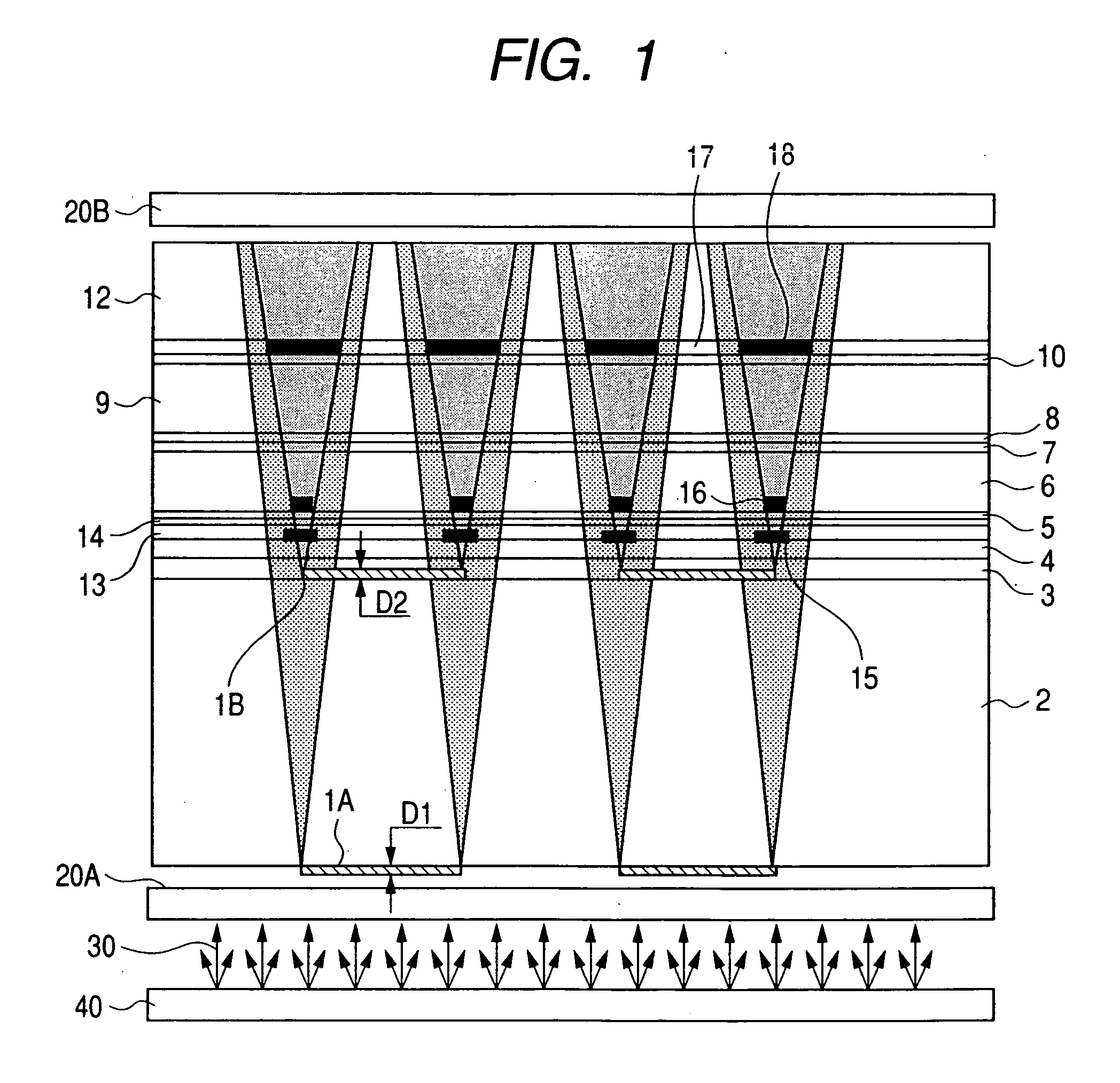
[0051]FIG. 2 is a schematic sectional view describing the second embodiment of the liquid crystal display apparatus according to the present invention. This liquid crystal display apparatus employs a so-called TN method (vertical electric field method). On the outer surface and inner surface of a glass substrate 2 as a first transparent substrate forming a thin-film transistor (TFT), phase shift elements 1A and 1B are formed. The phase shift element 1A on the outer surface is formed of an organic PAS film, with a refractive index of approximately 1.5. There is atmospheric air (with a refractive index of 1.0) between the phase shift elements 1A. A thickness D1 of this phase shift element 1A is set at 550 nm, a value obtained by substituting 550 nm for the center wavelength and 0.5 for Δn in D1Δn=center wavelength / 2.

[0052]On the other hand, the phase shift element 1B formed on the inner surface of the glass substrate 2 is an SiN layer (with a refractive index of approximately 2.0). As...

third embodiment

[0056]FIG. 3 is a sectional view describing the third embodiment of the liquid crystal display apparatus according to the present invention. The third embodiment is applied to a liquid crystal display panel of a semi-transmission liquid crystal display apparatus employing a TN method. In FIG. 3, for simplification, deflection plates 20A and 20B, and a back light system 40 are omitted from the illustration. In FIG. 3, this liquid crystal display is structured such that, in addition to illumination light from the back light system, external light Li entering from the color filter substrate 12 side passes through a color filter 17 and then through the layer of a liquid crystal 9, is reflected on a reflective plate 19, passes again through the layer of the liquid crystal 9 and then through the color filter 17, and exits to the outside as outgoing light Lo. In this case, the passage through the liquid crystal layer 9 twice requires that the thickness of the liquid crystal layer 9 at the ...


PUM

PropertyMeasurementUnit
wavelengthsaaaaaaaaaa
widthaaaaaaaaaa

Abstract

A phase shift element formed on the outer surface of a glass substrate is formed of an organic PAS film, with a refractive index of approximately 1.5. There is atmospheric air (with a refractive index of 1.0) between the phase shift elements. A thickness of the phase shift element is set at 550 nm, a value obtained by substituting 550 nm for a center wavelength and 0.5 for Δn in D1Δn=center wavelength / 2. A phase shift element formed on the inner surface of the glass substrate is an SiN layer (with a refractive index of approximately 2.0). A substance between the phase shift elements is a flattened film which has a heatproof temperature of 600 degrees centigrade or above, a low refractive index, and flattened effect. A thickness of the flattened film may be equal to or larger than a thickness of the phase shift element and thus is set at 550 nm. Through installation of the phase shift elements having a lens effect, light of a back light is efficiently condensed on an aperture part of a pixel, thereby improving the condensation efficiency at the aperture part and increasing an amount of light transmitted through a liquid crystal display panel.

Description

CLAIM OF PRIORITY[0001]The present application claims priority from Japanese application JP 2006-096764 filed on Mar. 31, 2006, the content of which is hereby incorporated by reference into this application.FIELD OF THE INVENTION[0002]The present invention relates to a transmitted light control structure which improves the energy efficiency by improving the light transmittance in a member having a light shielding part and a light transmitting part, and more specifically to a liquid crystal display apparatus realizing higher efficiency and higher luminance by use of a transmitted light control structure capable of achieving lower overall power consumption and higher luminance by increasing the use efficiency of illumination light of a planar shape.BACKGROUND OF THE INVENTION[0003]A structure that spatially and temporally controls the in-plane luminance distribution on a transparent substrate for light transmitted through the transparent substrate is useful for achieving higher lumina...

Claims


Application Information

Patent Timeline
Patent Type & Authority Applications(United States)
IPC IPC(8): G02F1/1335
CPCG02F1/133606G02F1/133526
Inventor TAKEDA, KAZUO
Owner HITACHI DISPLAYS
Why Eureka
Try Eureka