Nitride semiconductor device and manufacturing method thereof

a manufacturing method and semiconductor technology, applied in the direction of solid-state devices, semiconductor lasers, lasers, etc., can solve the problems of undesirable increase, inability to obtain low-resistance ohmic properties, and conventional manufacturing methods that cannot offer both satisfactory ohmic properties and satisfactory adhesion, etc., to achieve low-resistance ohmic properties and high adhesion

Active Publication Date: 2007-10-04
MITSUBISHI ELECTRIC CORP
View PDF2 Cites 48 Cited by
  • Summary
  • Abstract
  • Description
  • Claims
  • Application Information

AI Technical Summary

Benefits of technology

[0007]An object of the present invention is to provide a nitride semiconductor device and its manufacturing method which are capable of achieving low-resistance ohmic properties and high adhesion.
[0009]It is possible to achieve low-resistance ohmic properties and high adhesion between the nitride semiconductor substrate and the metal electrode layer.
[0011]It is possible to achieve low-resistance ohmic properties and high adhesion between the nitride semiconductor substrate and the metal electrode layer.

Problems solved by technology

However, such conventional manufacturing methods are incapable of offering both of satisfactory ohmic properties and satisfactory adhesion.
That is, in such methods, low-resistance ohmic properties cannot be obtained without application of high-temperature thermal treatment after the deposition of electrodes, or low-resistance ohmic properties can be obtained without thermal treatment but the resistance is undesirably increased by thermal treatment that is required for the device assembly process, or low-resistance ohmic properties can be obtained but sufficient adhesion cannot be obtained.
That is, the application of high-temperature thermal treatment may deteriorate electric characteristics of the device structure previously formed on the front side.
Also, improved adhesion may be obtained by designing specific electrode structures or by applying acid treatment to the surface, but it will impose restrictions on the processes or deteriorate the low resistance achieved by some means.

Method used


Image

  • Nitride semiconductor device and manufacturing method thereof
  • Nitride semiconductor device and manufacturing method thereof
  • Nitride semiconductor device and manufacturing method thereof

Examples


first preferred embodiment

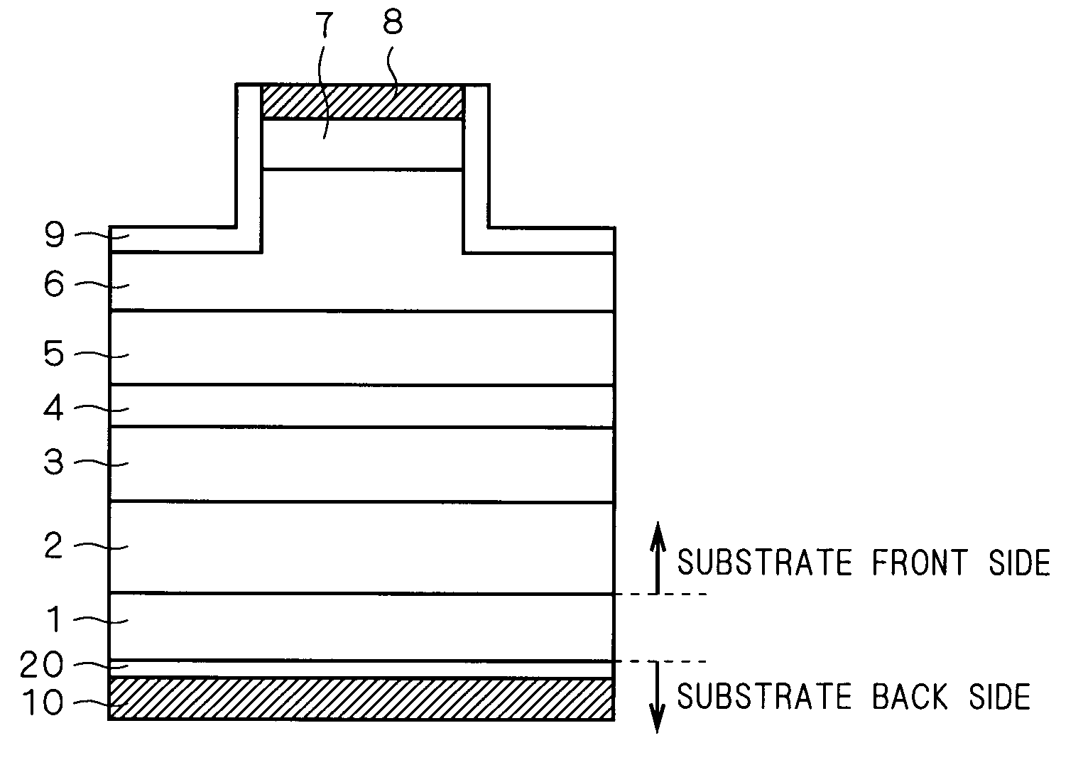
[0020]FIG. 1 is a diagram showing an example of the structure of a laser diode as a nitride semiconductor device according to a first preferred embodiment of the present invention. As shown in FIG. 1, the semiconductor device uses an n-type GaN substrate 1 as the nitride semiconductor substrate.

[0021]On the front surface side (a first main surface side), or the Ga surface, of the GaN substrate 1, an n-type AlGaN cladding layer 2, an n-type GaN guide layer 3, an active layer 4, a p-type GaN guide layer 5, a p-type AlGaN cladding layer 6, and a p-type GaN contact layer 7 are formed as a layered-structure of nitride semiconductors, and the GaN substrate 1 and the layered-structure form a laser diode element (a nitride semiconductor element). A p-electrode 8 is formed on the p-type GaN contact layer 7. The p-type AlGaN cladding layer 6 and the p-type GaN contact layer 7 are patterned in a given shape by etching. The p-electrode 8 is disposed on top of the p-type GaN contact layer 7. Als...

second preferred embodiment

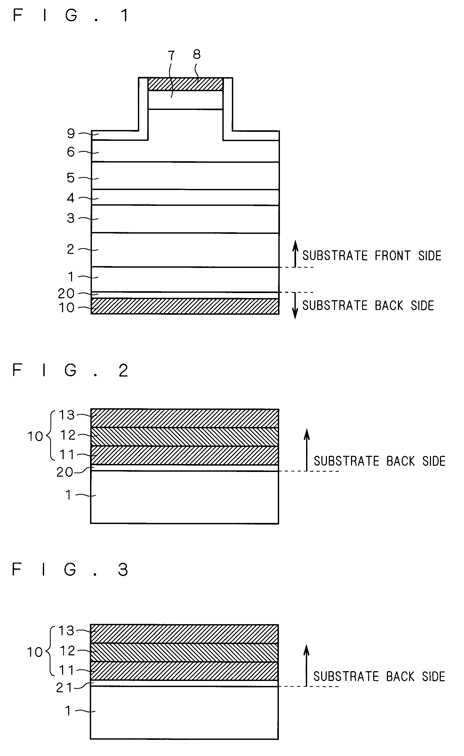
[0045]While the first preferred embodiment has described a structure in which the surface denatured layer 20 is interposed between the Ti film 11 and the GaN substrate 1 as shown in FIG. 2, a barrier layer may be further interposed between the Ti film 11 and the surface denatured layer 20.

[0046]FIG. 11 is an enlarged cross-sectional view showing the back surface side of the GaN substrate 1 of a nitride semiconductor device according to a second preferred embodiment. In FIG. 11, a barrier layer 30 for preventing the reaction between the n-electrode 10 and the surface denatured layer 20 is sandwiched between the n-electrode 10 (the Ti film 11) and the surface denatured layer 20 of FIG. 2.

[0047]The barrier layer 30 may be formed by applying a solution containing constituent material of the barrier layer 30 onto the GaN substrate 1, or by exposing it in an atmosphere containing constituent material of the barrier layer 30. The material of the barrier layer 30 can be organic-silicon-base...


PUM

PropertyMeasurementUnit
pHaaaaaaaaaa
particle sizeaaaaaaaaaa
roughnessaaaaaaaaaa

Abstract

A nitride semiconductor device and its manufacturing method are provided which are capable of achieving low-resistance ohmic properties and high adhesion. A nitride semiconductor device has an n-type GaN substrate over which a semiconductor element is formed and an n-electrode as a metal electrode formed over the back surface of the GaN substrate. A surface denatured layer functioning as a carrier supply layer is provided between the GaN substrate and the n-electrode. The surface denatured layer is formed by denaturing the back surface of the GaN substrate by causing it to react with a material that contains silicon.

Description

BACKGROUND OF THE INVENTION[0001]1. Field of the Invention[0002]The present invention relates to a nitride semiconductor device and a manufacturing method thereof, and particularly to a nitride semiconductor device having an n-electrode provided over the back surface of a nitride semiconductor substrate and a manufacturing method thereof.[0003]2. Description of the Background Art[0004]Methods of fabricating electrodes on nitride semiconductor substrates made of, e.g. GaN, are disclosed in Japanese Patent Publication No. 2967743 and Japanese Patent Application Laid-Open Nos. 2003-347660, 2004-6718 and 2005-268769 (hereinafter referred to respectively as Patent Documents 1 to 4), for example, in which the substrate is polished, further subjected to dry-etching for removal of polishing defects, or further subjected to oxygen plasma treatment. In the manufacturing method disclosed in Patent Document 4, a doping process is intentionally applied during the dry-etching.[0005]However, such ...

Claims


Application Information

Patent Timeline
Patent Type & Authority Applications(United States)
IPC IPC(8): H01L21/84
CPCH01S5/0206H01S5/0421H01S5/32341H01S5/22H01S5/0425H01S5/04252
Inventor KANAMOTO, KYOZOSHIOZAWA, KATSUOMIKAWASAKI, KAZUSHIGESAKUMA, HITOSHISUEHIRO, YOSHIYUKI
Owner MITSUBISHI ELECTRIC CORP
Why Eureka
Try Eureka