Nonvolatile ferroelectric memory

a ferroelectric memory and non-volatile technology, applied in the direction of digital storage, capacitors, instruments, etc., can solve the problems of slow operation speed of ferroelectric memory, inability to design a comparatively large layout size of the plate line drive circuit, and inability to flash memory to fewer commercial products

Active Publication Date: 2007-10-11
KIOXIA CORP
View PDF3 Cites 66 Cited by
  • Summary
  • Abstract
  • Description
  • Claims
  • Application Information

AI Technical Summary

Problems solved by technology

These shortages lead the flash memory to fewer commercial products as compared with the DRAM.
Furthermore, as a layout pitch of a plate line drive circuit becomes severe as comparable as the layout pitch of the word line, the layout size of the plate line drive circuit can not be designed comparatively large.
As a result, there was a shortage that an operation speed of the ferroelectric memory becomes slow.
However, realization of the memory cell having smaller size than 4F2 is principally difficult in the ferroelectric memory, even if these techniques are applied.
Therefore, ...

Method used


Image

  • Nonvolatile ferroelectric memory
  • Nonvolatile ferroelectric memory
  • Nonvolatile ferroelectric memory

Examples


first embodiment

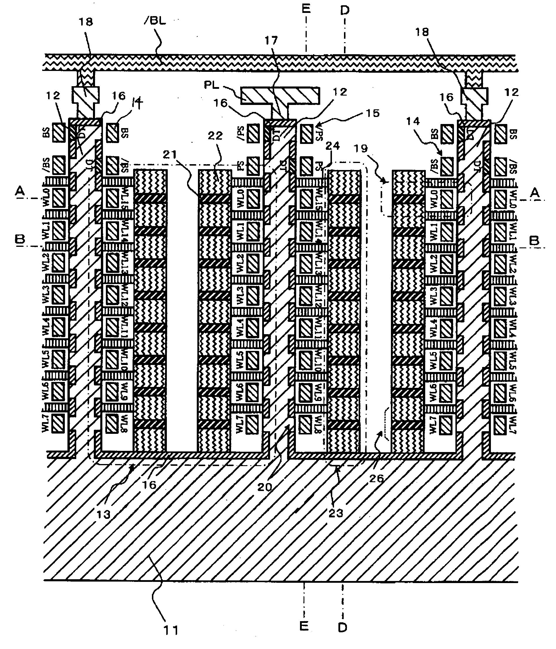
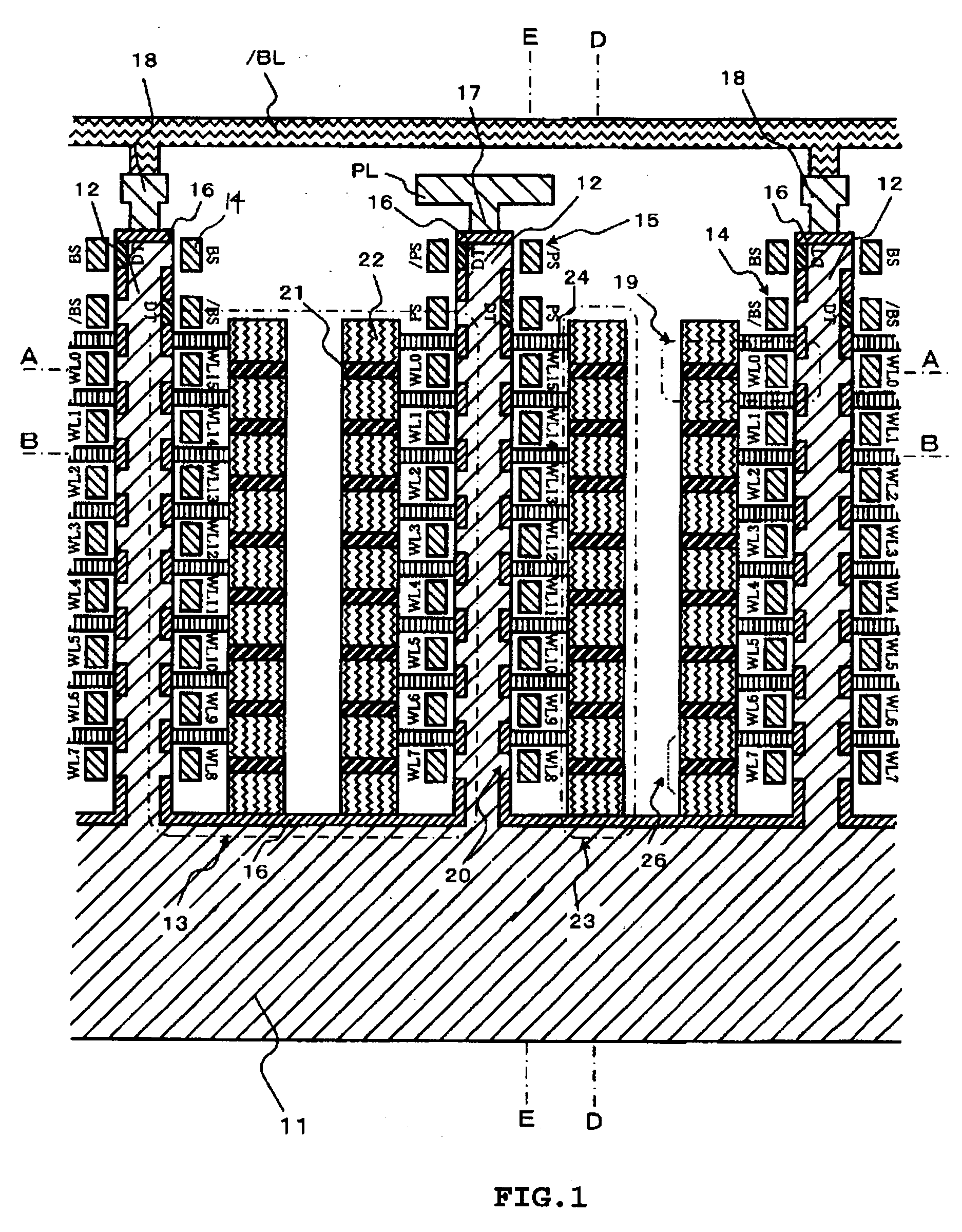
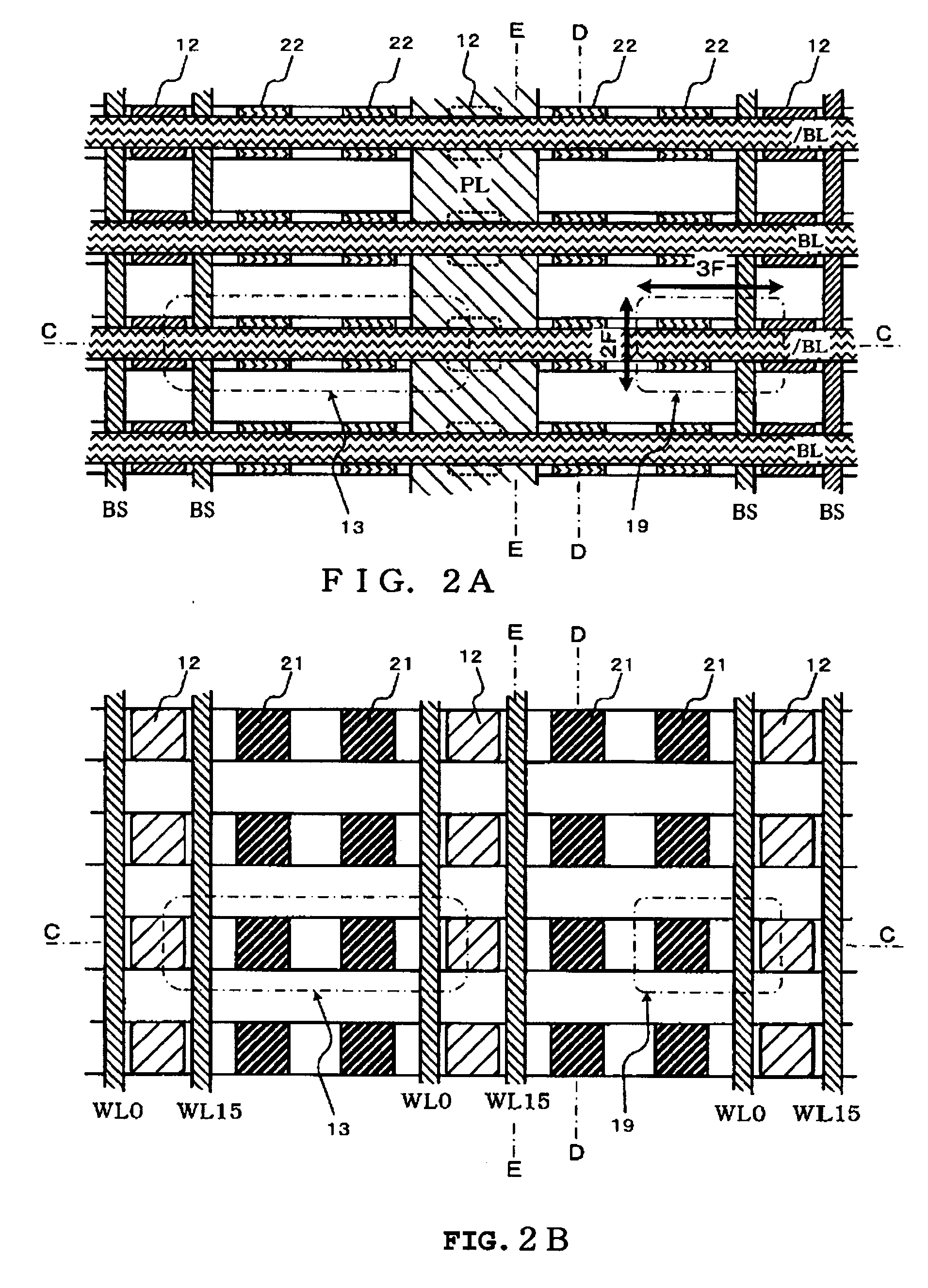
[0033]First, FIG. 1 is a cross-sectional view showing a memory cell portion of a nonvolatile ferroelectric memory according to a first embodiment of the present invention. Here, FIG. 1 mainly shows a memory cell block constituted of a plurality of ferroelectric memory cells and an interconnection portion related to accessing the memory. Further, a dielectric material of an interlayer dielectric film or the like is fluoroscopically illustrated with omitting description, such as hatching, for avoiding complication in the figure. The same description is also used on a cross-sectional view and a plane view as mentioned below.

[0034]The memory cell portion of the nonvolatile ferroelectric memory according to the first embodiment of the present invention includes a plurality of silicon pillars 12, each having a square pole shape. The silicon pillars 12 are formed on a main surface of a silicon substrate 11 at equal intervals. The memory cell portion has a plate line PL disposed over the si...

second embodiment

[0107]First, FIG. 10 is a cross-sectional view showing a memory cell portion of a nonvolatile ferroelectric memory according to a second embodiment of the present invention. Here, FIG. 10 mainly shows a memory cell block constituted of a plurality of ferroelectric memory cells and an interconnection portion related to accessing the memory. In FIG. 10, a portion of the same composition as the first embodiment is attached the same number.

[0108]The memory cell portion of the nonvolatile ferroelectric memory according to the second embodiment of the present invention includes a plurality of silicon pillars 12. The memory cell portion has the plate line PL disposed over the silicon pillars 12 along the word line (perpendicular to the page including FIG. 10), the bit line BL or / BL disposed over the plate line PL along orthogonal direction to the plate line PL (horizontal direction to the page including FIG. 10), the cell block 13 formed in a space between two of the silicon pillars 12 be...

third embodiment

[0116]First, FIG. 12 is a cross-sectional view showing a memory cell portion in a nonvolatile ferroelectric memory according to a third embodiment of the present invention. Here, FIG. 10 mainly shows a memory cell block constituted of a plurality of ferroelectric memory cells and an interconnection portion related to accessing the memories. In FIG. 10, a portion of the same composition as the first embodiment is attached the same number.

[0117]The memory cell portion of the nonvolatile ferroelectric memory according to the third embodiment of the present invention includes the plurality of silicon pillars 12. The memory cell portion has the bit line / BL over the silicon pillars 12 along perpendicular to the word line (horizontal direction to the page including FIG. 13), the plate lines PL and / PL disposed over the bit line BL along the word line (perpendicular direction to the page including FIG. 13), the cell block 13 formed in a space between two of the silicon pillars 12 being adj...


PUM


Abstract

According to an aspect of the invention, there is provided a nonvolatile ferroelectric memory, including a ferroelectric capacitor composed of a ferroelectric film sandwiched by capacitor electrodes made of a conductive material, a cell capacitor block stacked a plurality of the capacitor electrodes and the ferroelectric film of the ferroelectric capacitor perpendicular to a main surface of a silicon substrate in layer, a cell transistor having a drain electrode and a source electrode, the drain electrode and the source electrode are electrically connected to the ferroelectric capacitor in parallel, a memory cell composed of the ferroelectric capacitor and the cell transistor, a cell block having the plurality of memory cells electrically connected in series, the drain electrode and the source electrode being as a terminals, a word line, a bit line connected to one end of the cell block, the bit line being arranged along orthogonal direction to the word line and a plate line connected to the other end of the cell block, the plate line arranged along the word line.

Description

CROSS REFERENCE TO RELATED APPLICATION[0001]This application is based upon and claims the benefit of priority from the prior Japanese Application (No. 2006-105739, filed on Apr. 6, 2006), the entire contents of which are incorporated herein by reference.FIELD OF THE INVENTION[0002]The present invention relates to a nonvolatile ferroelectric memory, and in particular, to an arrangement of memory cells in the nonvolatile ferroelectric memory.DESCRIPTION OF THE BACKGROUND[0003]Today, a semiconductor memory is used in various commercial products, such as a main memory of both large-sized computer and personal computer, a home electric appliance, a cellular phone and the like. As a kind of semiconductor memory, a volatile DRAM (Dynamic RAM), a volatile SRAM (Static RAM), a nonvolatile MROM (Mask ROM), a nonvolatile flash EEPROM (flash memory) and the like have come out as a device product. Especially, the DRAM, in spite of the volatile memory, is superior to another memory from view poin...

Claims


Application Information

Patent Timeline
IPC IPC(8): G11C11/22
CPCG11C11/22H01L27/105H01L27/11502H01L28/55H01L27/11514H01L28/40H01L27/11507H10B53/20H10B53/30H10B53/00
Inventor TAKASHIMA, DAISABURO
Owner KIOXIA CORP
Why Eureka
Try Eureka