Modular electronic header assembly and methods of manufacture

a technology of electronic headers and modules, applied in the field of electronic and electronic elements, can solve the problems of inability to easily change the electrical configuration of a component, inability to efficiently handle manufacturing mistakes and inability to efficiently handle manufacturing errors or deficiencies in one or more. , to achieve the effect of improving manufacturability, improving reliability, and convenient soldering

Active Publication Date: 2007-10-11
PULSE ELECTRONICS
View PDF28 Cites 30 Cited by
  • Summary
  • Abstract
  • Description
  • Claims
  • Application Information

AI Technical Summary

Benefits of technology

[0032] In a sixth aspect of the invention, a method of attaching and interconnecting a substrate (e.g., PCB) and a device (e.g., modular assembly) is disclosed. In one embodiment, the method comprises using a single-step stencil print process to solder the pins of the assembly to the PCB, and to form a “bump” grid-array interconnect structure on the PCB. The bump grid-array interconnect method offers improved reliability over other prior art techniques (e.g., LGA or Land Grid Array) by increasing the component-to-PCB standoff (or standoff between the assembly and any intermediary component or substrate). It also offers improved manufacturability over an LGA or other such technique, as the bumps are essentially “pre-tinned” and easy to solder.

Problems solved by technology

Prior art techniques are unable to efficiently handle manufacturing mistakes or deficiencies in one or more of these channels, and often the entire component must be “scrapped” even though much of the circuit (e.g., multiple channels) functioned as designed.
No ability to change the electrical configuration of a component is readily provided under the prior art either.

Method used


Image

  • Modular electronic header assembly and methods of manufacture
  • Modular electronic header assembly and methods of manufacture
  • Modular electronic header assembly and methods of manufacture

Examples


second embodiment

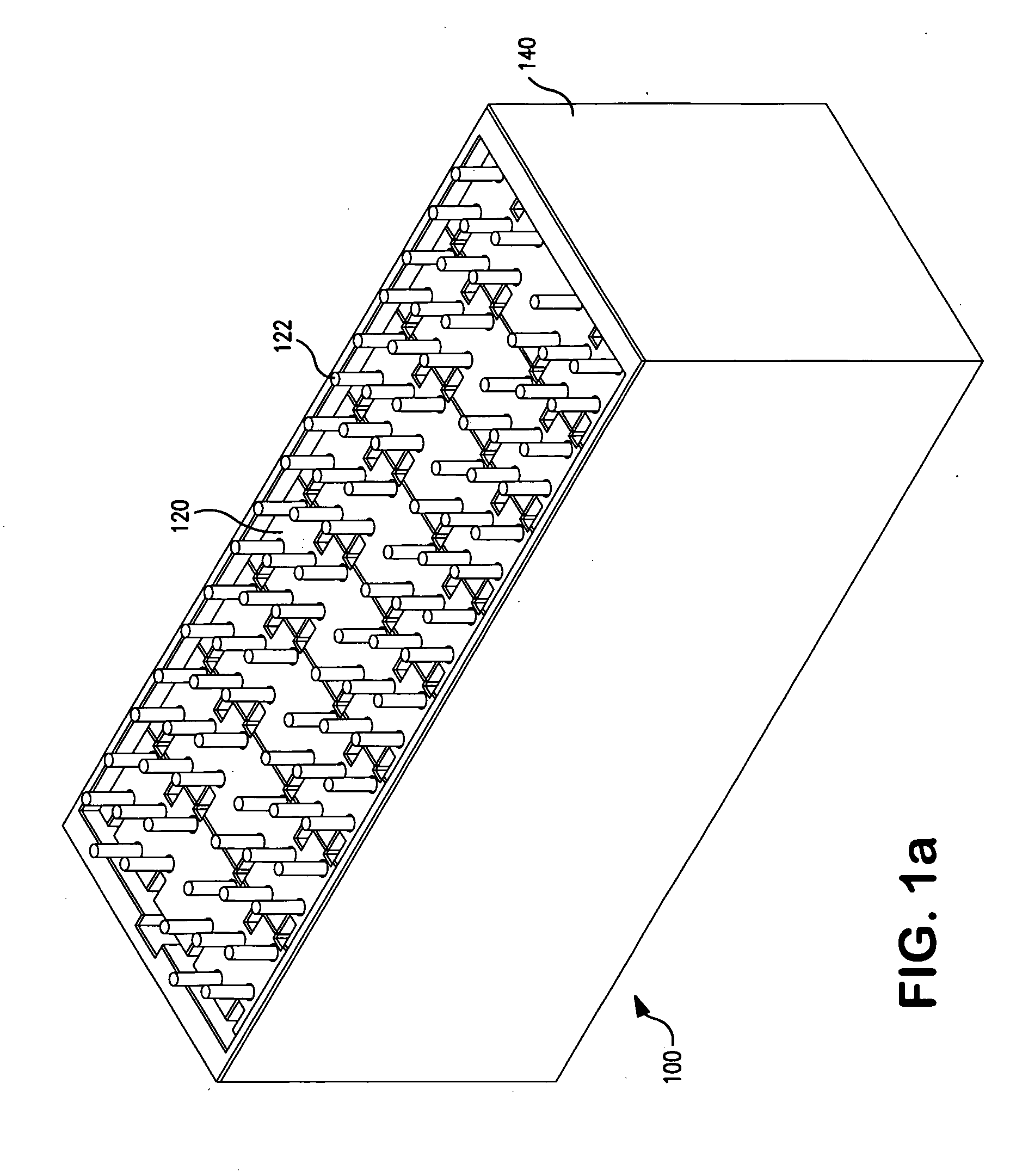
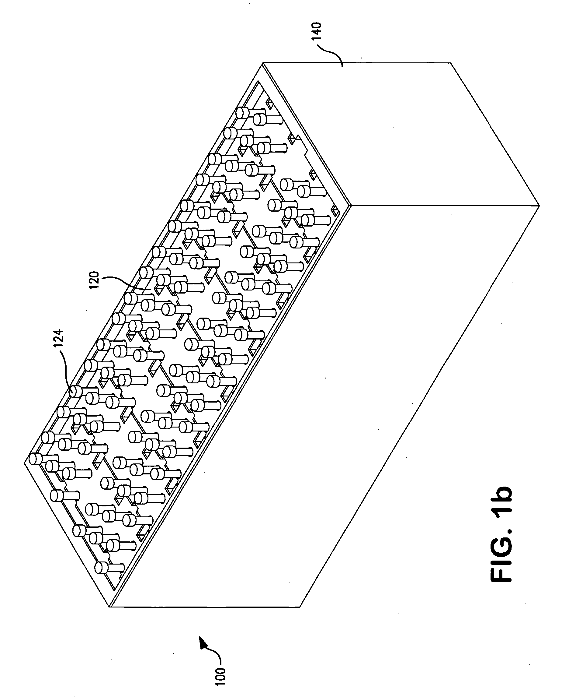
[0094] Referring now to FIG. 1b, the microminiature packaging device 100, generally similar to the device as shown in FIG. 1a is disclosed. The device 100 shown in FIG. 1b utilizes a spool head at the end of each pin 124, thereby providing more surface area and increasing the bond strength of the terminal array connection.

[0095] As is best illustrated in FIG. 1c, an exemplary embodiment of a modular header support elements 102 utilized in the embodiments of FIGS. 1a and 1b is shown. Each element 102 generally comprises a polymer material such as a high-temperature thermoset or thermoplastic polymer. The element 102 is advantageously manufactured by an injection-molding process, although other processes such as e.g., transfer molding or machining can be used if desired. The benefits of injection-molding are well understood in the polymer processing arts, and as such will not be discussed further herein. In one exemplary configuration, the element 102 is manufactured from a liquid cry...

third embodiment

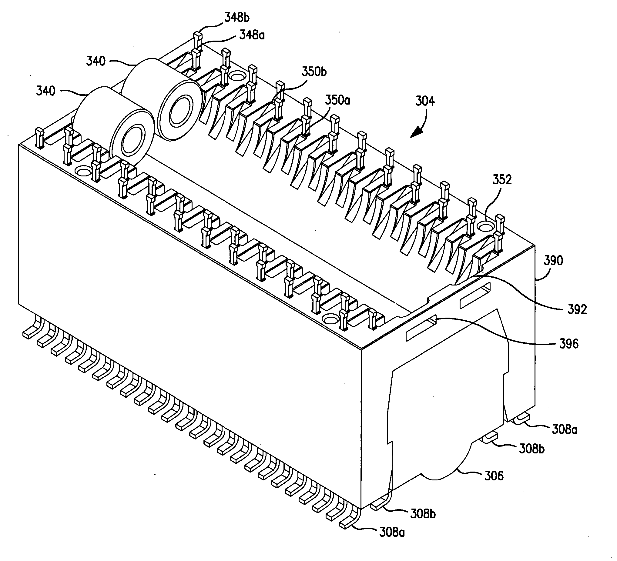
[0158] Referring now to FIG. 5, a vertically stacked header assembly device 500 according to the principles of the present invention is described. The device 500 of FIG. 5 comprises a lower header 506, upper header 504 and a cover 502. However, it should be noted that in this embodiment both the upper header 504 and the lower header 506 are essentially identical components with the terminology upper and lower merely reflecting the components respective positions with one another (and not any particular absolute position or orientation with respect to a parent device). The primary difference between the illustrated upper and lower headers is the positioning of the leads 508a and 508b within the header itself.

[0159] The device 500 comprises four (4) rows of through-hole leads 508a, 508b, each protruding from the bottom service of the upper and lower headers respectively. It is appreciated however, that the device 500 can be readily modified to accommodate surface mountable leads, simi...


PUM

PropertyMeasurementUnit
conductiveaaaaaaaaaa
non-conductiveaaaaaaaaaa
densitiesaaaaaaaaaa

Abstract

A device for electrically interconnecting and packaging electronic components. In one embodiment, a modular non-conducting base member having one or more component recesses and a plurality of lead channels formed therein is provided. At least one electronic component is disposed within the recess, and the wire leads of the component routed through the lead channels to a conductive lead terminal. A plurality of lead terminals, adapted to cooperate with the non-conducting base member, are received therein, and adapted to place the device in signal communication with an external printed circuit board. The modular non-conducting base members are assembled or stacked to form a unitary modular assembly. Methods for fabricating the device are also disclosed.

Description

1. FIELD OF THE INVENTION [0001] The present invention relates generally to electrical and electronic elements used in printed circuit board or other applications, and particularly to an improved package and method of packaging microminiature electronic components. 2. DESCRIPTION OF RELATED TECHNOLOGY [0002] For many years, electronic devices such as circuit boards have been fabricated by interconnecting a plurality of electronic components, both active and passive, on a planar printed circuit board. Typically, this printed circuit board has comprised an epoxy / fiberglass laminate substrate clad with a sheet of copper, which as been etched to delineate the conductive paths. Holes were drilled or formed through terminal portions of the conductive paths for receiving electronic component leads which were subsequently soldered thereto. [0003] So-called surface mount technology has evolved to permit more efficient automatic mass production of circuit boards with higher component densitie...

Claims


Application Information

Patent Timeline
Patent Type & Authority Applications(United States)
IPC IPC(8): H01R13/66
CPCH01F17/062H01F27/02H01F27/027H01F27/263H01F2038/006Y10T29/49004H05K3/303H05K7/10Y10T29/49002Y10T29/49144H02M1/126
Inventor GUTIERREZ, AURELIO J.MACHADO, RUSSELL L.SCHAFFER, CHRISRENTERIA, VICTOR H.
Owner PULSE ELECTRONICS
Why Eureka
Try Eureka