Superconductor components
- Summary
- Abstract
- Description
- Claims
- Application Information
AI Technical Summary
Benefits of technology
Problems solved by technology
Method used
Image
Examples
examples
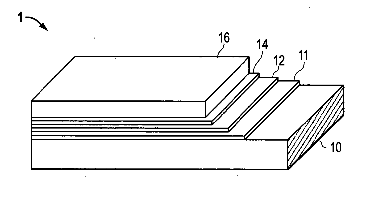
[0044] A Hastelloy C metal alloy substrate in the form of a tape having a thickness of ˜0.05 mm, length 250 m was polished to surface roughness of 1-5 nm Ra, then amorphous alumina of ˜70 nm was deposited on the metal alloy substrate by reactive ion beam sputtering of an Al metal target in a vacuum chamber at room temperature. During deposition, the tape translates from a feed spool, through a deposition zone in the form of a helix winding to make full use of large deposition area, then to a take-up spool. The Al target is then changed to a YSZ target, and sharply textured YSZ of ˜1000 nm is deposited on the amorphous alumina coated substrate by ion-beam assisted deposition (IBAD). The a lattice-match layer of CeO2 of ˜20 nm in thickness is grown epitaxially on the biaxially-textured YSZ by sputter or PLD method at high temperature, the YBCO superconducting film of 1-3 microns is deposited on the top of CeO2 by MOCVD. Then the tape is coated with silver of about 2-3 microns by DC sp...
PUM
 Abstract
Description
Claims
Application Information


