Semiconductor apparatus and method of producing the same

Inactive Publication Date: 2007-10-18
SHARP KK
View PDF5 Cites 27 Cited by
  • Summary
  • Abstract
  • Description
  • Claims
  • Application Information

AI Technical Summary

Benefits of technology

[0023]With this structure, the inner side surface of the through hole is covered by the second insulating film, and the second insulating film insulates the conductive wiring and the semiconductor substrate from each other. This prevents the inner side surface of the through hole of the semiconductor substrate from exposing. Therefore, insulation between the conductive wiring and the semiconductor substrate in the through hole is prevented from deteriorating, so that leakage due to deterioration in the insulation is prevented. Further, with the structure, only the insulating film on the bottom surface of the through hole is eliminated even when the side surface of the through hole is formed at an angle of 90 degrees with respect to the bottom surface of the through hole. This allows the semiconductor apparatus to be reduced in size.
[0024]To attain the above object, the method of producing a semiconductor apparatus in accordance with the present invention is adapted so that the method includes the steps of: forming an electrode pad on a first surface of a semiconductor substrate via a first insulating film; forming a through hole in the semiconductor substrate from a second surface, which is positioned opposite to the first surface, of the semiconductor substrate to the electrode pad formed on the first surface; forming a second insulating film on a side surface of the through hole, on a bottom surface of the through hole, and on the second surface of the semiconductor substrate to insulate the semiconductor substrate from a conductive wiring; eliminating the second insulating film formed so as to overlap the bottom surface of the through hole, and forming a connection opening to the electrode pad in such a way as to avoid a periphery of the bottom surface of the through hole; and forming the conductive wiring to electrically connect the electrode pad to an external connection terminal.
[0025]With this structure, only a part of the second insulating film placed on the bottom surface of the through hole is eliminated, which part is not in contact with a periphery of the bottom surface of the through hole. The part from which the second insulating film is eliminated is used as a connection opening. This assures that the connection opening is surrounded by the second insulating film. This allows the conductive wiring and the semiconductor substrate to be isolated from each other.
[0026]Further, to attain the above object, the method of producing a semiconductor apparatus in accordance with the present invent

Problems solved by technology

However, a semiconductor apparatus employing this conventional through electrode and a method of producing the through electrode have a problem that steps that are difficult to control and extremely complicated are required to form a through electrode that is highly insulative.
For example, the first way has a problem that, when the resist is applied evenly to the second surface of the semiconductor substrate having the through hole, it is difficult to bury the resist evenly into the through hole.
For example, when a through hole of 70 μm square is formed in a semiconductor substrate having a thickness of 200 μm, it is difficult to apply the resist evenly into this very small through hole.
Even if the resist is buried evenly in the through hole, it is difficult to eliminate the resist in the through hole by developing because, with the hole of this aspect ratio, developing fluid flown into the hole is less likely to circulate.
However, there is a problem that, when the second insulating film is formed by forming an oxide film inside of the through hole by CVD, the second insulating film formed on the side surface of the through hole becomes thinner than the second insulating film formed on the second surface of the semiconductor substrate.
Another problem is that, when anisotropic etching is carried out on the second insulating film formed on the rear

Method used


Image

  • Semiconductor apparatus and method of producing the same
  • Semiconductor apparatus and method of producing the same
  • Semiconductor apparatus and method of producing the same

Examples


embodiment 1

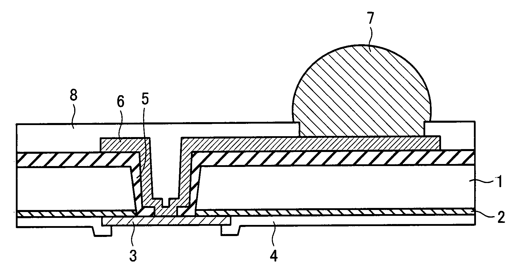
[0071]FIG. 1 is a cross section showing a structure of the vicinity of an electrode section of a semiconductor apparatus in accordance with the present embodiment.

[0072]As shown in FIG. 1, in the semiconductor apparatus of the present embodiment, a metal wiring layer of single-layer or multi-layer (generally multi-layer) is formed on a first surface (front surface) of a semiconductor substrate 1 via a first insulating film 2. Although not shown in the figure, a semiconductor device is connected to a predetermined terminal on the metal wiring layer. An electrode pad 3 is formed for the semiconductor device to receive and supply a signal. FIG. 1 only shows the electrode pad 3, which is included in the metal wiring layer. A protection film 4 made of an oxide film or a nitride film is formed on the metal wiring layer. Materials of the semiconductor substrate 1 are not particularly limited, and any publicly-known substrates may be used. For example a Si-substrate or a GaAs-substrate may ...

embodiment 2

[0098]The following describes a semiconductor apparatus of the present embodiment. Structures other than those described in the present embodiment are same as those of Embodiment 1. For convenience in description, components having the same functions as those of the components shown in the figures of Embodiment 1 are given the same reference numerals, and description thereof is omitted.

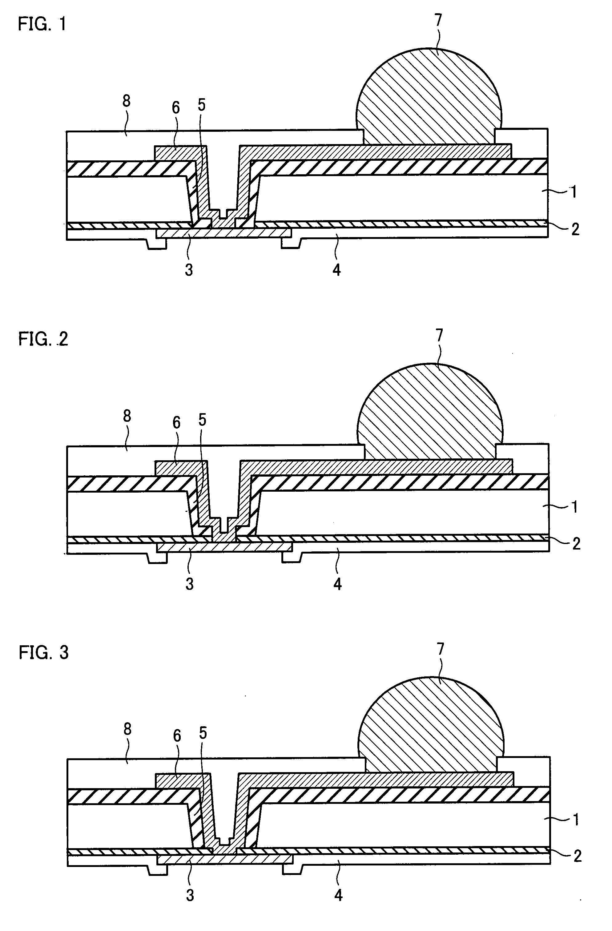
[0099]FIG. 2 is a cross section of a structure of the vicinity of an electrode section of a semiconductor apparatus of another embodiment of the present invention.

[0100]As shown in FIG. 2, in the semiconductor apparatus of the present embodiment, a through electrode is formed in an area where an electrode pad 3 is formed. Accordingly, in a semiconductor substrate 1, a through hole is formed immediately above the electrode pad 3. A second insulating film 5 is formed to cover a side surface of the through hole and a second surface of the semiconductor substrate 1. Further, a first insulating film 2 and ...

embodiment 3

[0110]The following describes a semiconductor apparatus of the present embodiment. Structures other than those described in the present embodiment are same as those of Embodiment 1. For convenience in description, components having the same functions as those of the components shown in the figures of Embodiment 1 are given the same reference numerals, and description thereof is omitted.

[0111]FIG. 3 is a cross section of a structure of the vicinity of an electrode section of a semiconductor apparatus in accordance with another embodiment of the present invention.

[0112]As shown in FIG. 3, in the semiconductor apparatus of the present embodiment, a through electrode is formed in an area where an electrode pad 3 is formed. Accordingly, in a semiconductor substrate 1, a through hole is formed immediately above the electrode pad 3. The second insulating film 5 is formed to cover the side surface of the through hole and a second surface of the semiconductor substrate 1. The first insulatin...


PUM


Abstract

A semiconductor apparatus including: a semiconductor substrate having a through hole; an electrode pad provided on a first surface of the semiconductor substrate so as to cover the through hole; an external connection terminal provided on a second surface of the semiconductor substrate; a conductive wiring passing through the through hole and allowing conduction between the electrode pad and an external connection terminal; a first insulating film provided on the first surface of the semiconductor substrate; and a second insulating film provided on a second surface of the semiconductor substrate and on an inner surface of the through hole to insulate the semiconductor substrate from the conductive wiring; the conductive wiring being connected to the electrode pad via the connection opening formed in at least one of the first insulating film and the second insulating film that are formed in such a way that at least a part of the first insulating film and a part of the second insulating film overlap, in a direction vertical to the first surface of the semiconductor substrate, the bottom surface of the through hole, and the connection opening being formed so as to avoid a periphery of the bottom surface of the through hole. This provides a semiconductor apparatus with a highly-reliable through electrode and a method of producing the apparatus.

Description

[0001]This Nonprovisional application claims priority under 35 U.S.C. § 119(a) on Patent Applications No. 112779 / 2006 filed in Japan on Apr. 14, 2006, and No. 345014 / 2006 filed in Japan on Dec. 21, 2006, the entire contents of which are hereby incorporated by reference.FIELD OF THE INVENTION[0002]The present invention relates to a semiconductor apparatus and a method of producing the semiconductor apparatus. Particularly, the present invention relates to a semiconductor apparatus including a conductive wiring suitably isolated with an insulating film, and a method of producing the semiconductor apparatus.BACKGROUND OF THE INVENTION[0003]Demands for smaller and thinner semiconductor apparatus have been increasing in recent years. Laminates of a plurality of semiconductor apparatuses have been widely employed to increase mounting density. In response to such demands, for example the technique disclosed in Patent Document 1 (Japanese Unexamined Patent Publication No. 2003-309221; publi...

Claims


Application Information

Patent Timeline
IPC IPC(8): H01L23/48
CPCH01L21/76898H01L23/3114H01L2224/16H01L27/14683H01L27/14618H01L24/02H01L24/03H01L24/05H01L2224/0231H01L2224/02372H01L2224/02377H01L2224/05001H01L2224/05008H01L2224/05009H01L2224/05022H01L2224/05024H01L2224/051H01L2224/05548H01L2224/05647H01L2224/13024H01L2224/13025H01L2924/0001H01L2924/00014H01L2224/02H01L23/12H01L23/52
Inventor IDA, TOHRU
Owner SHARP KK
Why Eureka
Try Eureka