Liquid crystal device and electronic apparatus

a liquid crystal device and electronic equipment technology, applied in non-linear optics, instruments, optics, etc., can solve the problems of reduced transmittance, level of image signals, and short circuit of common and pixel electrodes, so as to reduce thickness and facilitate formation

Active Publication Date: 2007-10-18
JAPAN DISPLAY WEST
View PDF13 Cites 19 Cited by
  • Summary
  • Abstract
  • Description
  • Claims
  • Application Information

AI Technical Summary

Benefits of technology

[0016] In some embodiments of a liquid crystal device, the first and second transparent electrodes preferably do not overlap at positions corresponding to the contact holes. Therefore, even if the second insulating layer serving as a dielectric layer has a extremely small thickness, portions of the first and second transparent electrodes that are located in the contact holes can be prevented from being short-circuited. This allows the second insulating layer to have a small thickness without causing a reduction in yield. Therefore, auxiliary capacitors can be readily formed using the second insulating layer and the level of image signals can be reduced by generating fringe fields having high intensity. In other words, the second insulating layer is allowed to have a small thickness without causing a reduction in yield; hence, the auxiliary capacitors have high capacitance and fringe fields generated between the first and second transparent electrodes have high intensity. This allows molecules of the liquid crystals to be readily operated.
[0018] This is effective in preventing the first and second transparent electrodes from overlapping at the positions corresponding to the contact holes. Hence, the first and second transparent electrode portions located in the contact holes can be prevented from being short-circuited.
[0025] In order to prevent the above problems, the counter substrate can include the light-shielding layer as described above. Therefore, even if the liquid crystal molecules present in regions located near the first or second lines or the notches are misaligned, these regions can be covered with the light-shielding layer. Therefore, display quality can be prevented from being deteriorated due to the misalignment of the liquid crystal molecules.

Problems solved by technology

Hence, there is a problem in that liquid crystal molecules located above the pixel electrodes cannot be sufficiently driven and this causes a reduction in transmittance.
The FFS-mode liquid crystal devices have a problem that when an insulating layer located between common electrodes and pixel electrodes has a reduced thickness such that auxiliary capacitors can be readily formed using the insulating layer and such that the level of image signals can be reduced by increasing the intensity of electric fields generated between the common and pixel electrodes, the common and pixel electrodes can be short-circuited depending on the layout of the common and pixel electrodes.
Since the second transparent electrodes have the notches, portions of an alignment layer that are located near the notches cannot be sufficiently rubbed depending on the shape of the notches.
Therefore, the liquid crystal molecules located above the insufficiently rubbed portions thereof cannot be aligned in the rubbing direction of the alignment layer.
During the operation of the liquid crystal, voltages are differently applied to the liquid crystal molecules depending on whether the liquid crystal molecules are located above the insufficiently rubbed portions thereof or sufficiently rubbed portions thereof; hence, the liquid crystal molecules cannot be properly controlled in alignment.
This can have an adverse effect on display quality.

Method used


Image

  • Liquid crystal device and electronic apparatus
  • Liquid crystal device and electronic apparatus
  • Liquid crystal device and electronic apparatus

Examples


first embodiment

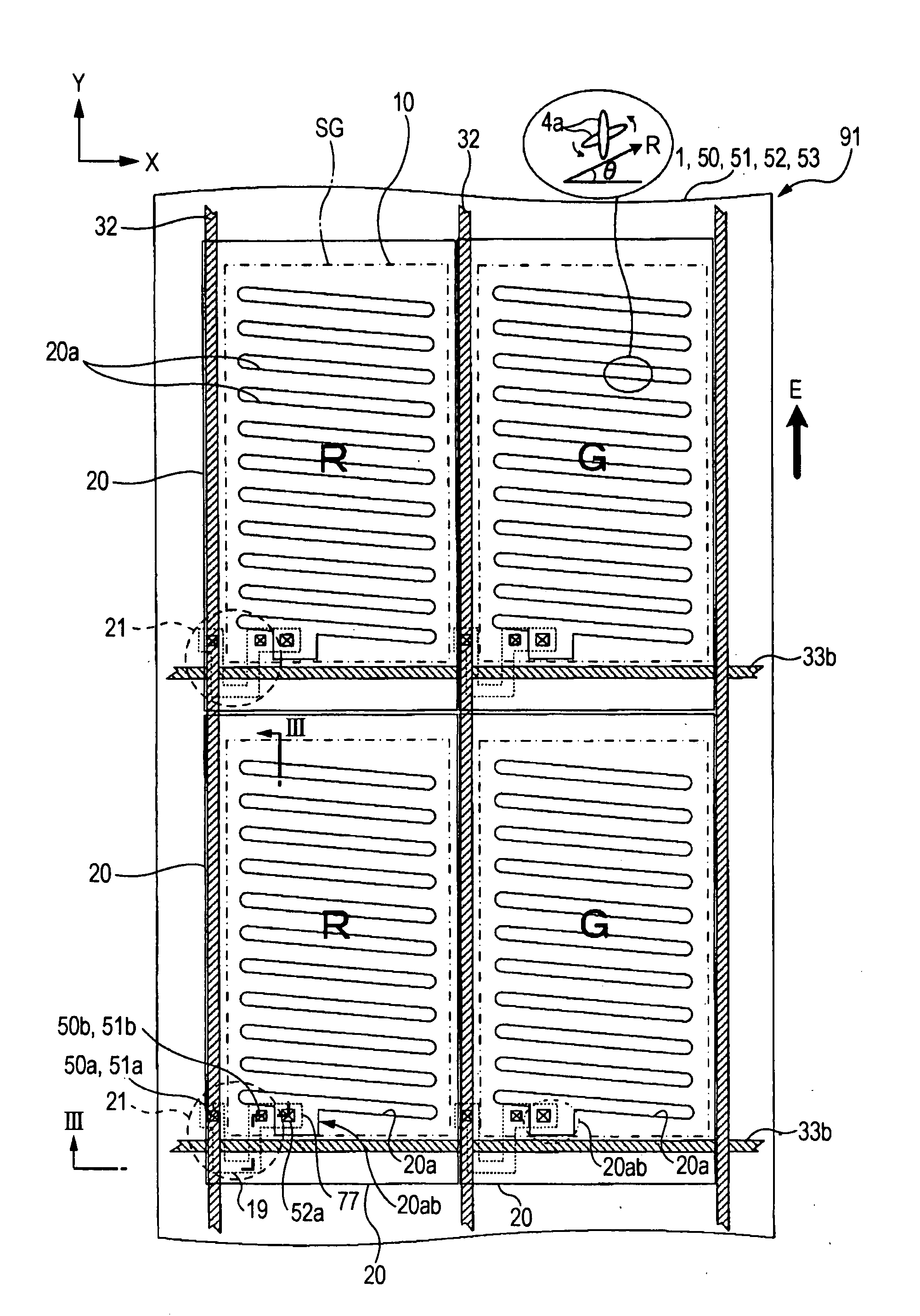
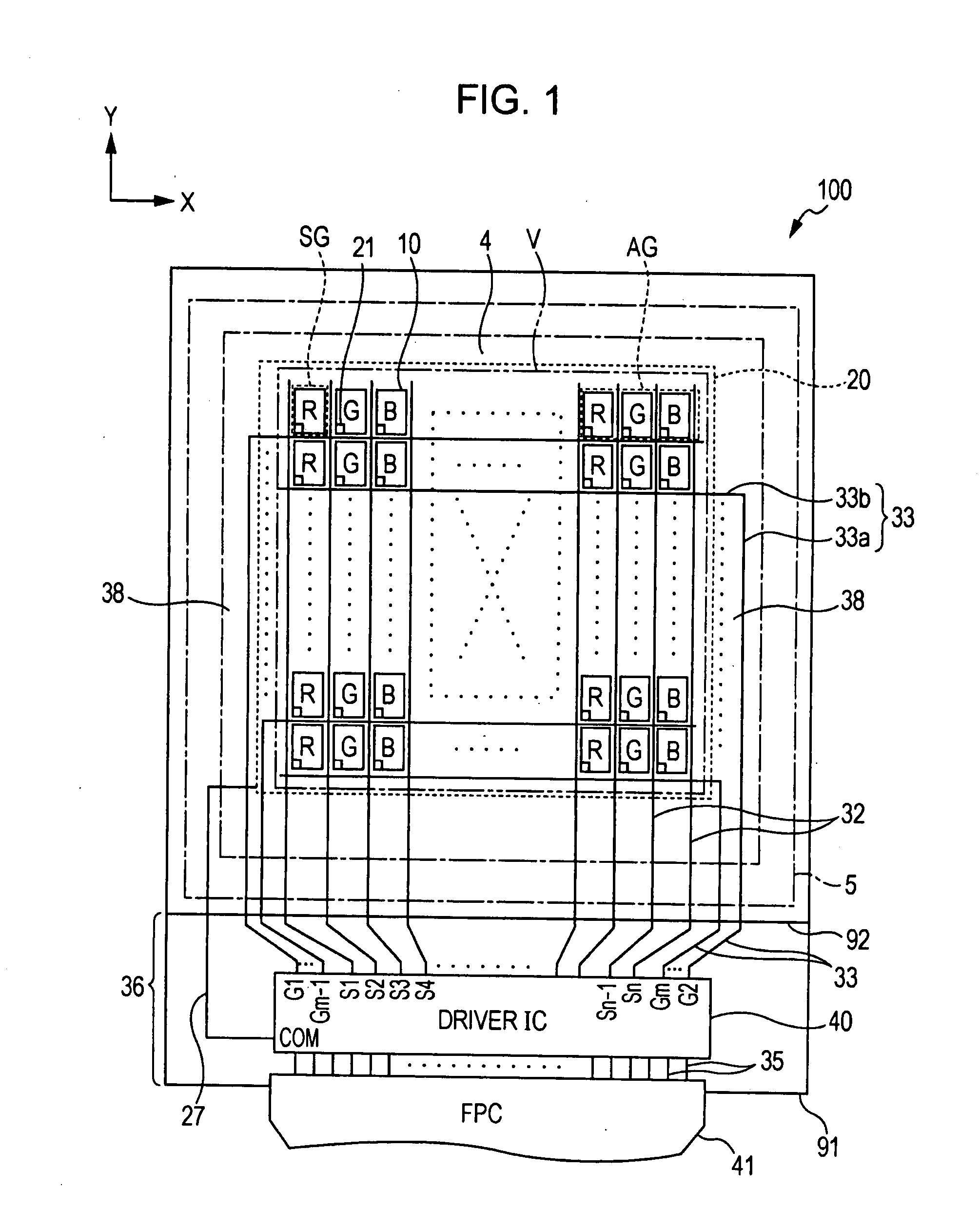
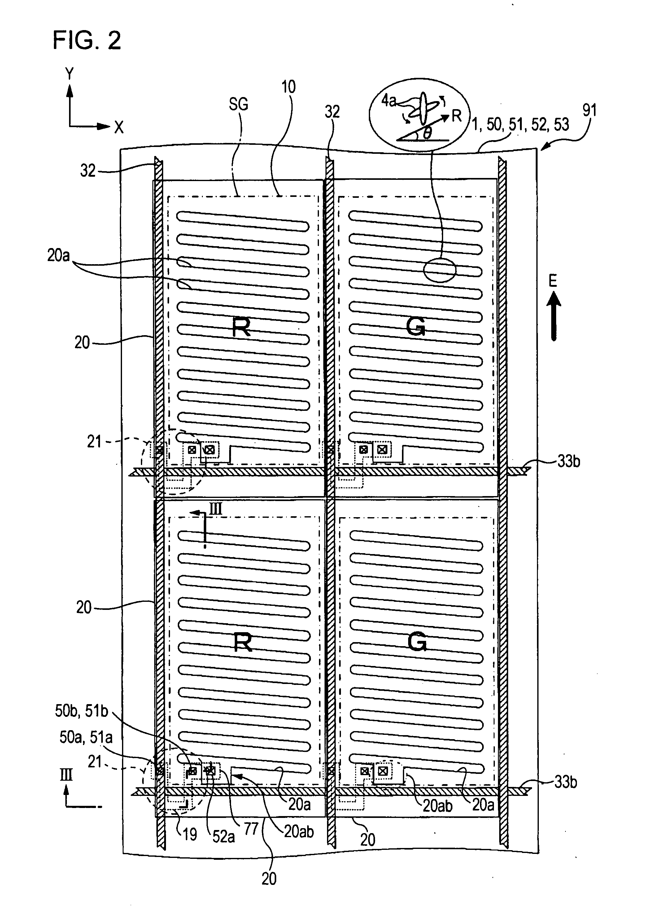
[0037] A liquid crystal device 100 according to a first embodiment of the present invention will now be described with reference to FIG. 1.

[0038]FIG. 1 shows the liquid crystal device 100 in plan view. With reference to FIG. 1, a color filter substrate 92 is located close to an observer and an element substrate 91 is located far from the observer. The vertical or column direction in FIG. 1 is defined as a Y direction and the horizontal or row direction in FIG. 1 is defined as an X direction. R, G, and B represent red subpixel regions, green subpixel regions, and blue subpixel regions, respectively. The red, green, and blue subpixel regions R, G, and B are each referred to as subpixel regions SG Pixel regions AG each consists of one red subpixel region R, green subpixel region G, and blue subpixel region B arranged in a row. One display region present in each subpixel region SG can hereinafter be referred to as a subpixel and one display region corresponding to each pixel region AG ...

second embodiment

[0080] A liquid crystal device 200 according to a second embodiment of the present invention will now be described with reference to FIGS. 6 and 7.

[0081]FIG. 6 shows four pixels in plan view. The pixels are included in an element substrate 91, included in the liquid crystal device 200, having a configuration similar to that described in the first embodiment. FIG. 6 also shows principal components included in a color filter substrate 94 included in the liquid crystal device 200. FIG. 7 shows a principal part of the liquid crystal device 200 in cross section taken along the line VII-VII of FIG. 6. In particular, FIG. 7 shows one subpixel in cross section taken along a line extending through one of LTPS-TFTs 21 included in the liquid crystal device 200.

[0082] The liquid crystal device 200 of this embodiment is different from the liquid crystal device 100 of the first embodiment in that the color filter substrate 94 of this embodiment has a configuration different from that of the col...

third embodiment

[0096] A third embodiment of the present invention provides an electronic apparatus. The electronic apparatus includes the liquid crystal device 100 or 200 according to the first or second embodiment, incorporated as a functional part of the electronic apparatus. Examples of the electronic apparatus will now be described with reference to FIGS. 8A and 8B.

[0097]FIG. 8A shows a portable personal computer that is an example of the electronic apparatus in perspective view. The personal computer is a so-called notebook-type one. With reference to FIG. 8A, the personal computer is represented by reference numeral 710 and includes a main body 712 including a keyboard 711 and also includes a display section 713 including a panel. The panel includes the liquid crystal device 100 or 200 of the first or second embodiment.

[0098]FIG. 8B shows a mobile phone that is another example of the electronic apparatus in perspective view. With reference to FIG. 8B, the mobile phone is represented by ref...


PUM

PropertyMeasurementUnit
temperatureaaaaaaaaaa
capacitanceaaaaaaaaaa

Abstract

A liquid crystal device includes a substrate for holding a liquid crystal. The substrate includes switching elements, a first insulating layer which overlies the switching elements and which has contact holes located at positions corresponding to the switching elements, first transparent electrodes which overlie the first insulating layer and which are electrically connected to the switching elements through the contact holes, a second insulating layer overlying the first transparent electrodes, and second transparent electrodes which overlie the second insulating layer and which each have a plurality of slits for generating electric fields between the first and second transparent electrodes, the second transparent electrodes not overlapping the contact holes in plan view.

Description

CROSS-REFERENCE TO RELATED APPLICATION [0001] This application claims priority from Japanese Patent Application No. 2006-070997, filed in the Japanese Patent Office on Mar. 15, 2006, the entire disclosure of which is hereby incorporated by reference in its entirety. BACKGROUND [0002] 1. Technical Field [0003] Embodiments of the present invention relate to a liquid crystal device for displaying various types of information and also relate to an electronic apparatus including the liquid crystal display. [0004] 2. Related Art [0005] Examples of liquid crystal display modes include twisted nematic (TN) modes, vertical alignment modes for achieving a wide viewing angle and a high contrast ratio, transverse electric field modes such as an in-plane switching (IPS) mode and a fringe field switching (FFS) mode. [0006] In the EPS mode, electric fields are applied to liquid crystal molecules in parallel to substrates. The IPS mode is superior to the TN mode in that a wide viewing angle can be ...

Claims


Application Information

Patent Timeline
Patent Type & Authority Applications(United States)
IPC IPC(8): G02F1/1343
CPCG02F1/136227G02F1/134363G02F1/1343G02F1/136
Inventor FUJITA, SHINKOIDE, SHIN
Owner JAPAN DISPLAY WEST
Why Eureka
Try Eureka