

Methods for controllable doping of aluminum nitride bulk crystals
a technology of bulk crystals and aluminum nitride, which is applied in the direction of crystal growth process, after-treatment details, condensed vapors, etc., can solve the problems of difficult to achieve reasonable conductivity levels, difficult to create donor or acceptor levels with dopants, and wide-bandgap aln crystals with a tendency to form charge-compensating vacancy defects, etc., to achieve less active, reduce density, and avoid local strain
- Summary
- Abstract
- Description
- Claims
- Application Information
AI Technical Summary
Benefits of technology
Problems solved by technology
Method used
Image

Examples
Embodiment Construction
Brief Summary of the Invention
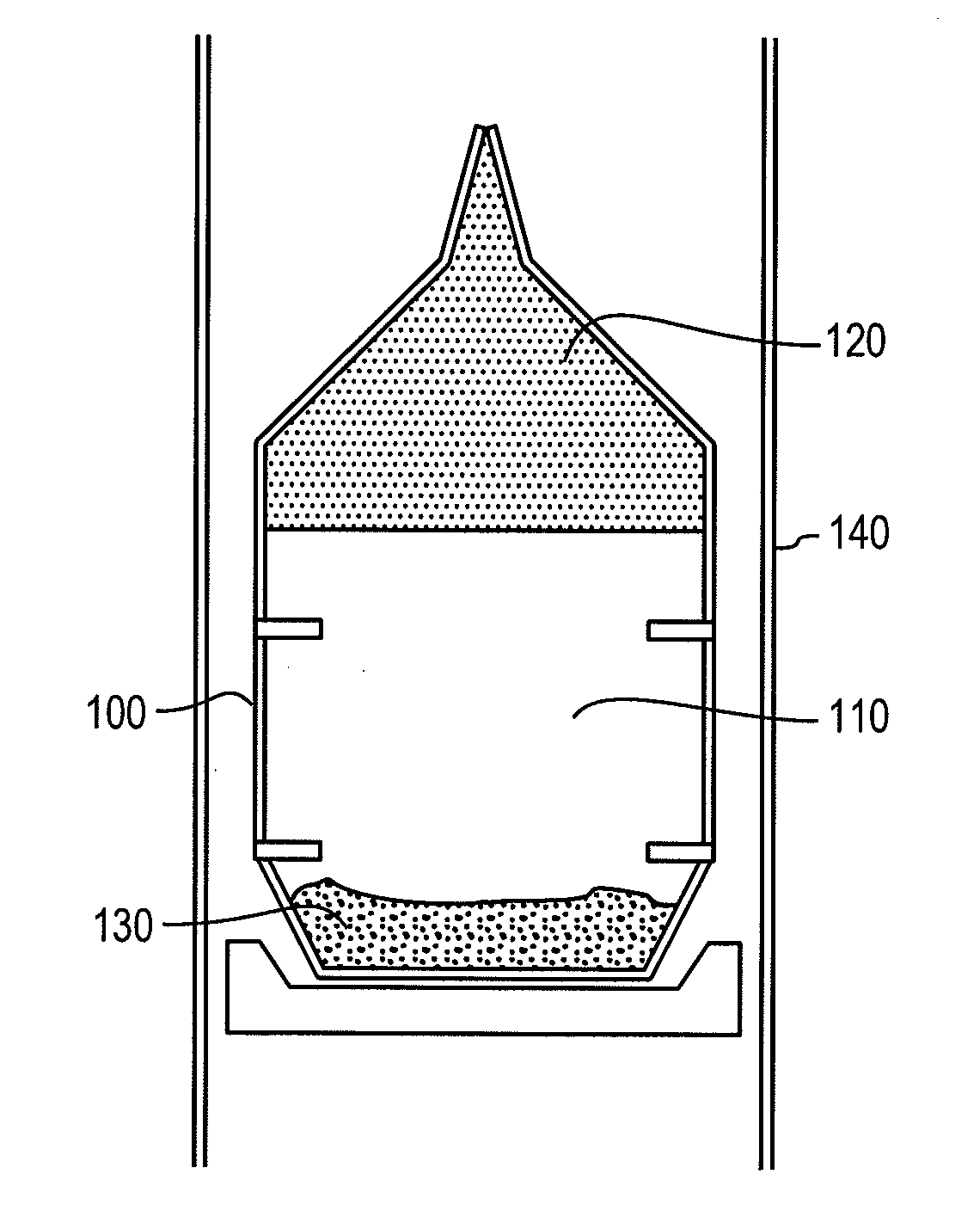
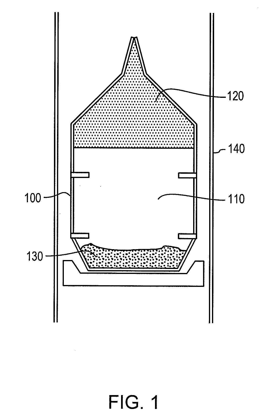
[0006] In accordance with the present invention, a donor or acceptor level is created within the perfect, stoichiometric AlN or AlxGa1-xN (where 0≦x≦1, herein sometimes referred to as AlGaN) lattice by introducing a substitutional impurity that has greater or fewer electrons than aluminum (Al) or nitrogen (N). Charge-compensating defects, such as vacancies on the Al cation site (designated as VAl) or the N anion site (designated as VN) or impurities with deep levels which will trap the free charge created by the doping impurity, are desirably avoided but, more generally, are either reduced in density or less active. In order to use atoms that have nearly the same diameter as Al or N and avoid local strain, dopants are preferably selected from the upper part of the periodic table. Choices for the Al site include beryllium (Be), magnesium (Mg), zinc (Zn), carbon (C), and silicon (Si) while C, Si, and oxygen (O) are possible choices for the N site. Dopant...
PUM
| Property | Measurement | Unit |
|---|---|---|
| pressure | aaaaa | aaaaa |
| pressure | aaaaa | aaaaa |
| temperature | aaaaa | aaaaa |
Abstract
Description
Claims
Application Information