Low-temperature metal-induced crystallization of silicon-germanium films

US20070246764A1Active Publication Date: 2007-10-25SANDISK TECH LLC

Image

  • Low-temperature metal-induced crystallization of silicon-germanium films
  • Low-temperature metal-induced crystallization of silicon-germanium films
  • Low-temperature metal-induced crystallization of silicon-germanium films

Examples


Embodiment Construction

[0004] The present invention is defined by the following claims, and nothing in this section should be taken as a limitation on those claims. In general, the invention is directed to crystallization of a deposited silicon-germanium alloy film.

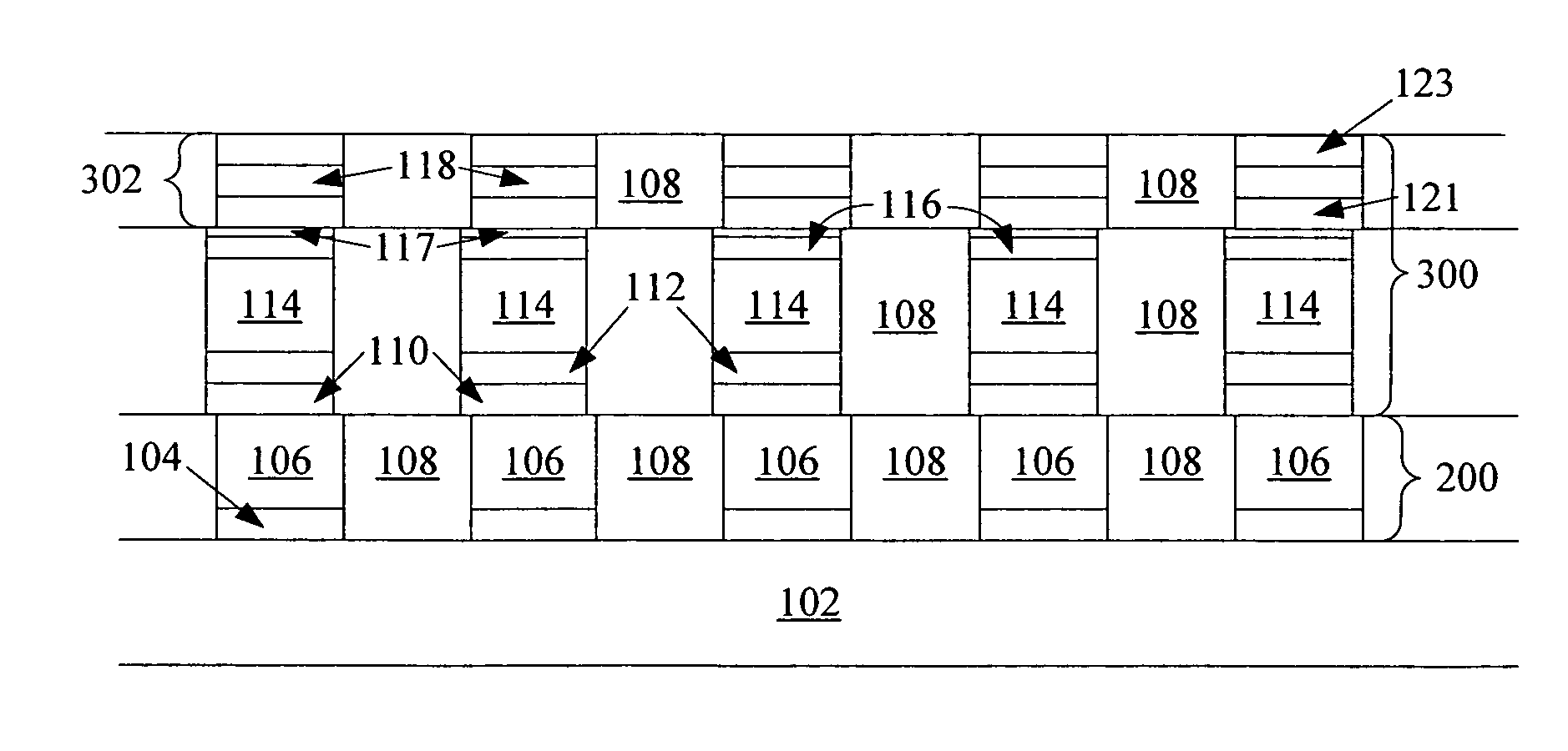
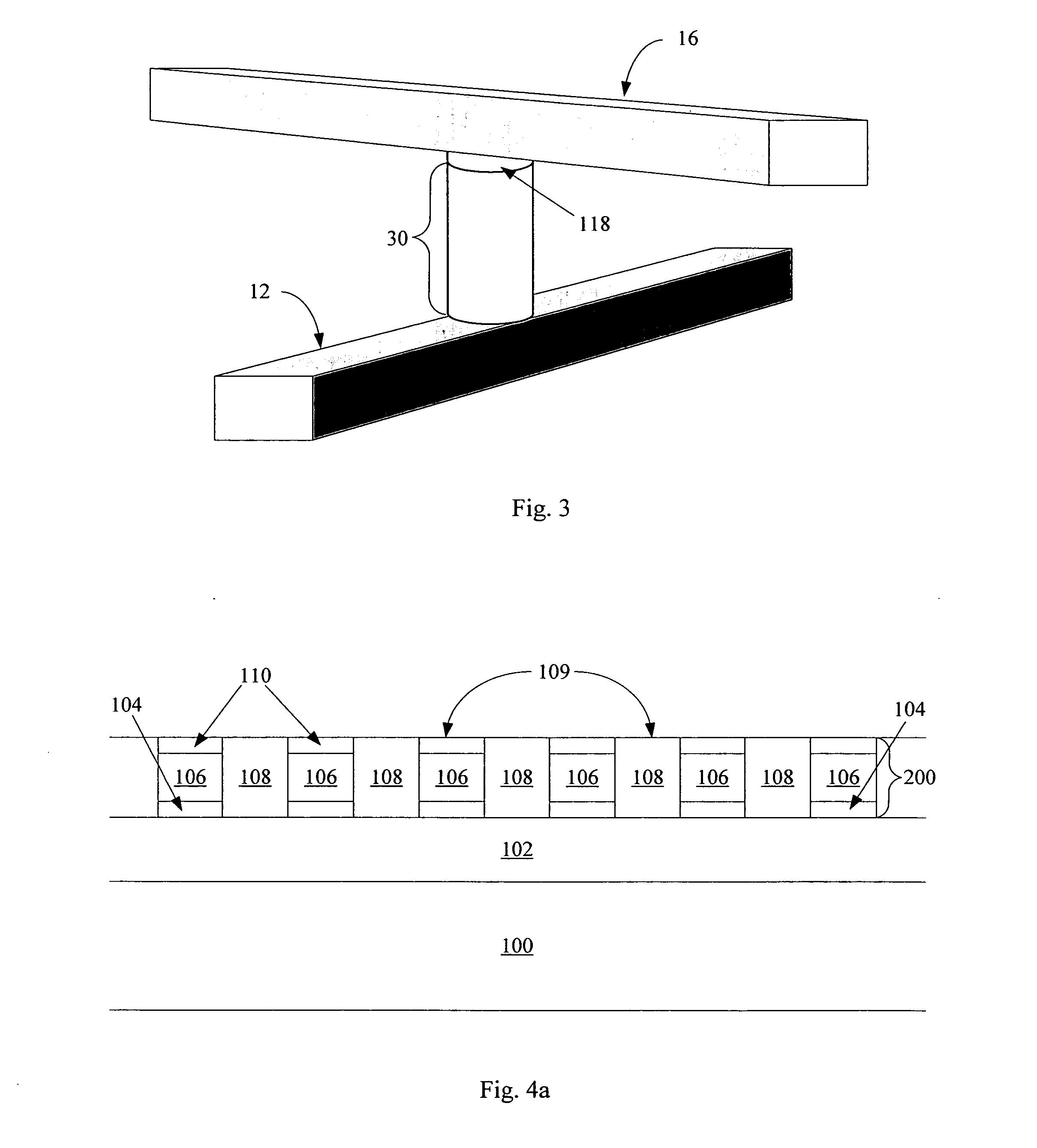
[0005] A first aspect of the invention provides for a method for crystallizing a semiconductor film, the method comprising: depositing a film of a silicon-germanium alloy at a temperature below about 490 degrees C.; depositing a layer of a metal catalyst selected from the group consisting of nickel, cobalt, ruthenium, and aluminum, the metal catalyst in contact with the silicon-germanium film; and crystallizing the silicon-germanium alloy film at a temperature below about 490 degrees C.

[0006] A preferred embodiment of the present invention provides for a method for forming a first memory level comprising a plurality of first memory cells, the method comprising: depositing a film of a silicon-gernanium alloy at a temperature below about 490 de...


PUM

PropertyMeasurementUnit
Fractionaaaaaaaaaa
Fractionaaaaaaaaaa
Percent by atomaaaaaaaaaa

Abstract

The present invention provides for a low-temperature method to crystallize a silicon-germanium film. Metal-induced crystallization of a deposited silicon film can serve to reduce the temperature required to crystallize the film. Increasing germanium content in a silicon-germanium alloy further decreases crystallization temperature. By using metal-induced crystallization to crystallize a deposited silicon-germanium film, temperature can be reduced substantially. In preferred embodiments, for example in a monolithic three dimensional array of stacked memory levels, reduced temperature allows the use of aluminum metallization. In some embodiments, use of metal-induced crystallization in a vertically oriented silicon-germanium diode having conductive contacts at the top and bottom end is be particularly advantageous, as increased solubility of the metal catalyst in the contact material will reduce the risk of metal contamination of the diode.

Description

BACKGROUND OF THE INVENTION [0001] The invention relates to a low-temperature method to crystallize a silicon-germanium film. [0002] The relatively high temperature required to crystallize deposited semiconductor materials such as silicon and silicon-germanium alloys can have adverse effects on semiconductor devices. High temperatures can lead to unwanted diffusion of dopants, can cause peeling due to differential expansion and contraction of unlike materials during thermal cycles, and can prohibit the use of desirable conductive materials like aluminum which have low thermal tolerance. These disadvantages are particularly acute in monolithic three dimensional memory arrays, in which a memory level formed above a substrate will be exposed to the temperatures required to form additional memory levels stacked above it. [0003] There is advantage, therefore, in lowering the temperature required to crystallize deposited semiconductor material. SUMMARY OF THE PREFERRED EMBODIMENTS [0004] ...

Claims


Application Information

Patent Timeline
25 Oct 2007
Publication
US20070246764A1
IPC
H01L29/94
CPC
C30B1/00; C30B29/52; H01L21/02532; H01L21/02672; H01L23/5252; H01L27/1021; Y10S148/059; H01L29/66136
Inventors
HERNER, S. BRAD