Delay locked loop

a delay and loop technology, applied in the field of digital duty cycle correction circuits of delay locked loops, can solve the problems of high accuracy of dcc circuits, large area, high power consumption, etc., and achieve the effect of maintaining excellent performance and minimizing power consumption and area

Active Publication Date: 2007-10-25
SK HYNIX INC
View PDF11 Cites 21 Cited by
  • Summary
  • Abstract
  • Description
  • Claims
  • Application Information

AI Technical Summary

Benefits of technology

[0006]Accordingly, the present invention addresses the above problems, and discloses a duty correction circuit, in which it can correct the duty of an output pulse, minimize power consumption

Problems solved by technology

The analog DCC circuit is high in accuracy, but is difficult to implement for high-speed operation, whereas the digita

Method used


Image

  • Delay locked loop
  • Delay locked loop
  • Delay locked loop

Examples


Embodiment Construction

[0014]Now, specific embodiments according to the present patent will be described with reference to the accompanying drawings.

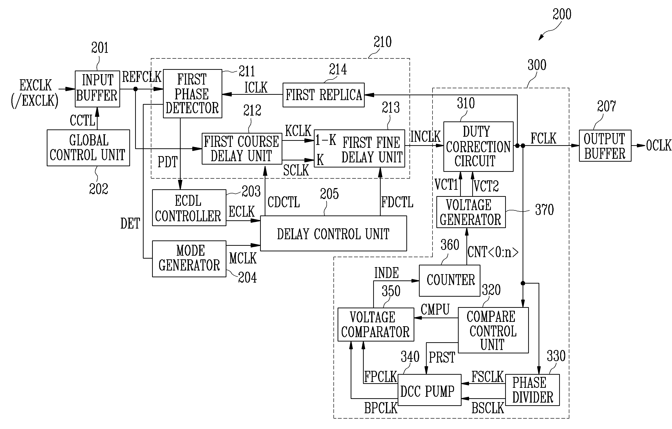
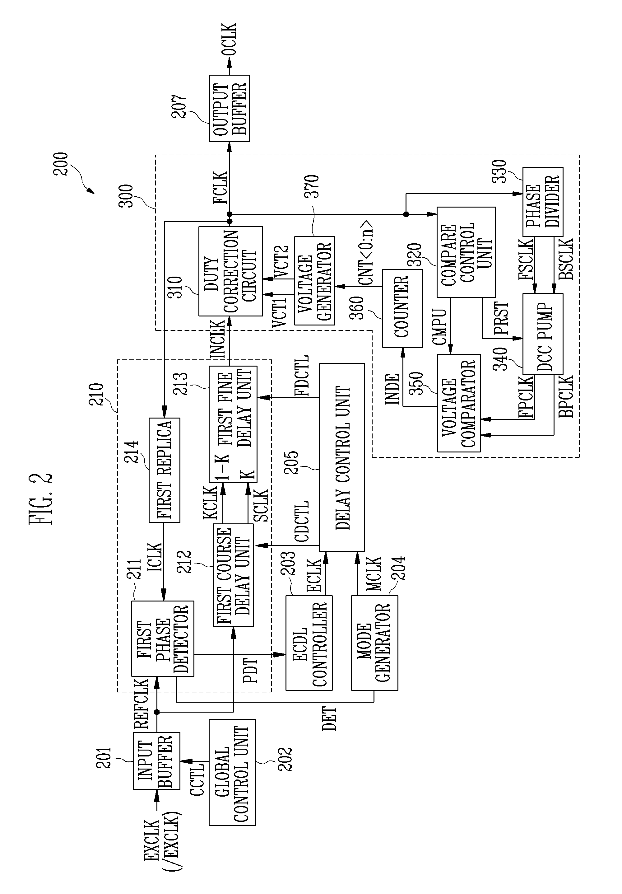
[0015]FIG. 2 is a schematic block diagram of a DLL according to the present invention. The DLL 200 includes an input buffer 201, a global control unit 202, a delay unit 210, an ECDL controller 203, a mode generator 204, a delay control unit 205, a duty correction unit 300 and an output buffer 207. The delay unit 210 includes a first phase detector 211, a first coarse delay unit 212, a first fine delay unit 213 and a first replica 214. The duty correction unit 300 includes a duty correction circuit 310, a compare control unit 320, a phase divider 330, a DCC pump 340, a voltage comparator 350, a counter 360 and a voltage generator 370. The input buffer 201 receives an external clock EXCLK and outputs a reference clock REFCLK. The global control unit 202 generates a global clock signal CCTL that is periodically toggled. The first phase detector 211 compares the ...


PUM


Abstract

The digital duty cycle correction circuit according to the present invention includes a first conversion circuit for buffering an internal clock output from a delay locked loop (DLL), converting the buffered internal clock into first and second clocks through first and second terminals, delaying the second clock according to voltage supplied to the second terminal through a capacitor, converting the delayed second clock into a first signal, and converting the first clock into a third clock, which rises at a falling edge of the first clock and falls at a rising edge of the first signal; and a second conversion circuit for converting the third clock into an output clock, which rises at a falling edge of the third clock and falls at a rising edge of the third clock.

Description

CROSS-REFERENCES TO RELATED APPLICATIONS[0001]The present application claims priority to Korean patent application number 10-2006-036608, filed on Apr. 24, 2006, which is incorporated by reference in its entirety.BACKGROUND OF THE INVENTION[0002]The present invention relates to a digital duty cycle correction circuit of a Delay Locked Loop (DLL).[0003]In general, in DDR SDRAM, the input and output operations of data are performed at the rising and falling edges of a clock in synchronization with an external clock. The data output by the read operation must be identical to the timing of the rising and falling edges of an external clock. Therefore, it is required that a circuit within the DDR SDRAM receive the external clock and control the output of the data by generating an internal clock that is delayed for a given time. The circuit generating the internal clock includes a DLL or a Phase Locked Loop (PLL). Furthermore, although the ratio of a duty high pulse and a duty low pulse of...

Claims


Application Information

Patent Timeline
IPC IPC(8): H03K3/017
CPCH03K5/1565G11C5/145G11C7/222G11C11/4076H03L7/0812
Inventor CHO, KWANG JUNKU, KIE BONG
Owner SK HYNIX INC
Why Eureka
Try Eureka