Manufacturing method of organic electroluminescence element

Inactive Publication Date: 2007-10-25
DAI NIPPON PRINTING CO LTD
View PDF6 Cites 26 Cited by
  • Summary
  • Abstract
  • Description
  • Claims
  • Application Information

AI Technical Summary

Benefits of technology

[0020]Using of the material having a liquid repellent functional group for the charge injecting and transporting layer or applying of the liquid repellent process to the charge injecting and transporting layer enables the present invention to achieve the effect of obtaining a good wettability change. Moreover, since the photocatalyst is contained in the photocat

Problems solved by technology

However, in the method of patterning an organic EL layer using a photocatalyst, the surface state of the layer containing the photocatalyst may become rough because the photocatalyst such as titanium oxide is granular shape.
Accordingly, obstacles present between the light emitting layer and the layer containing the photocatalyst become large to disturb the charge transfer.
As a recult, a problematic decline in the light emission characteristics maybe ca

Method used


Image

  • Manufacturing method of organic electroluminescence element
  • Manufacturing method of organic electroluminescence element
  • Manufacturing method of organic electroluminescence element

Examples


first embodiment

I. First Embodiment

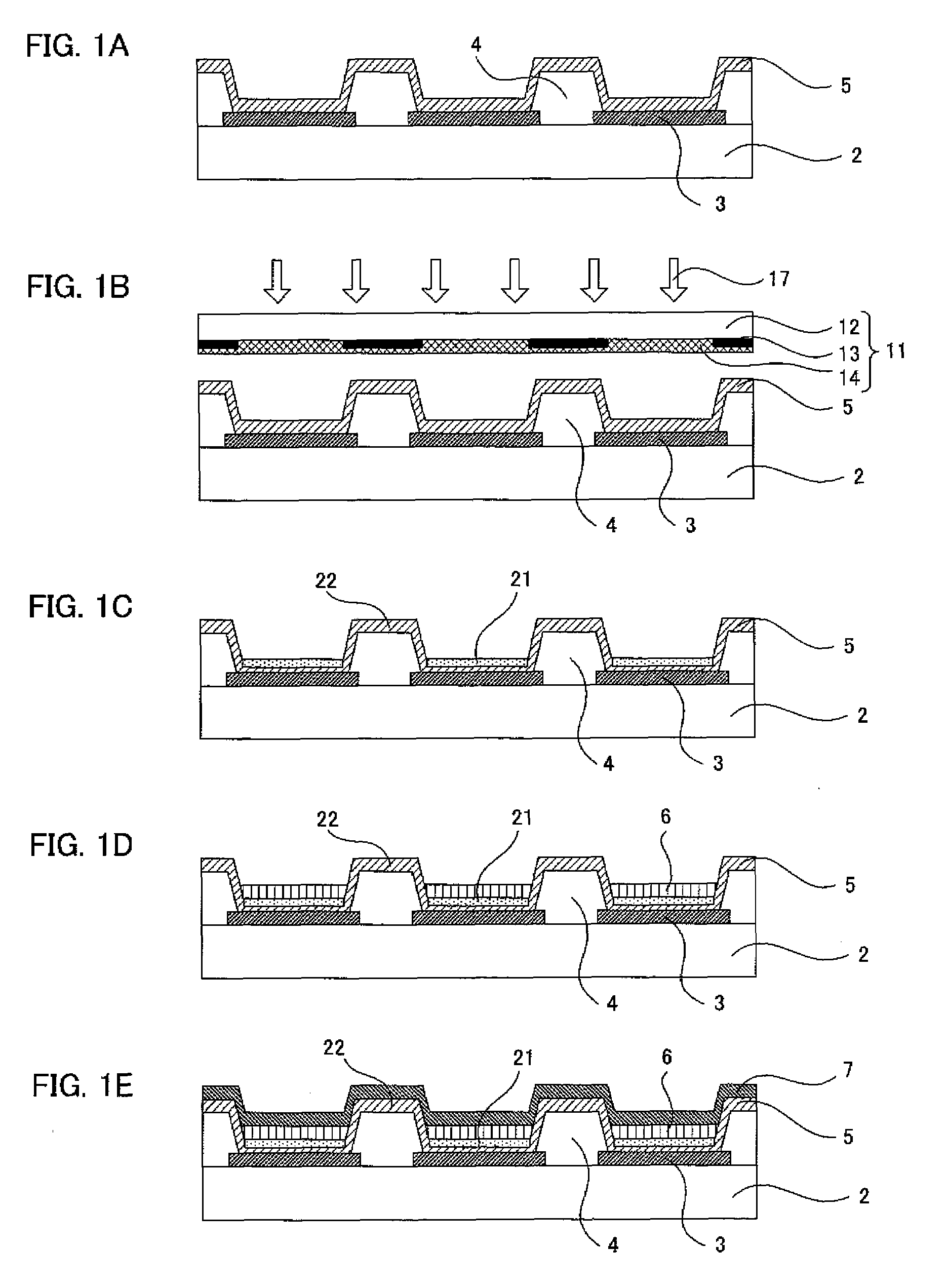
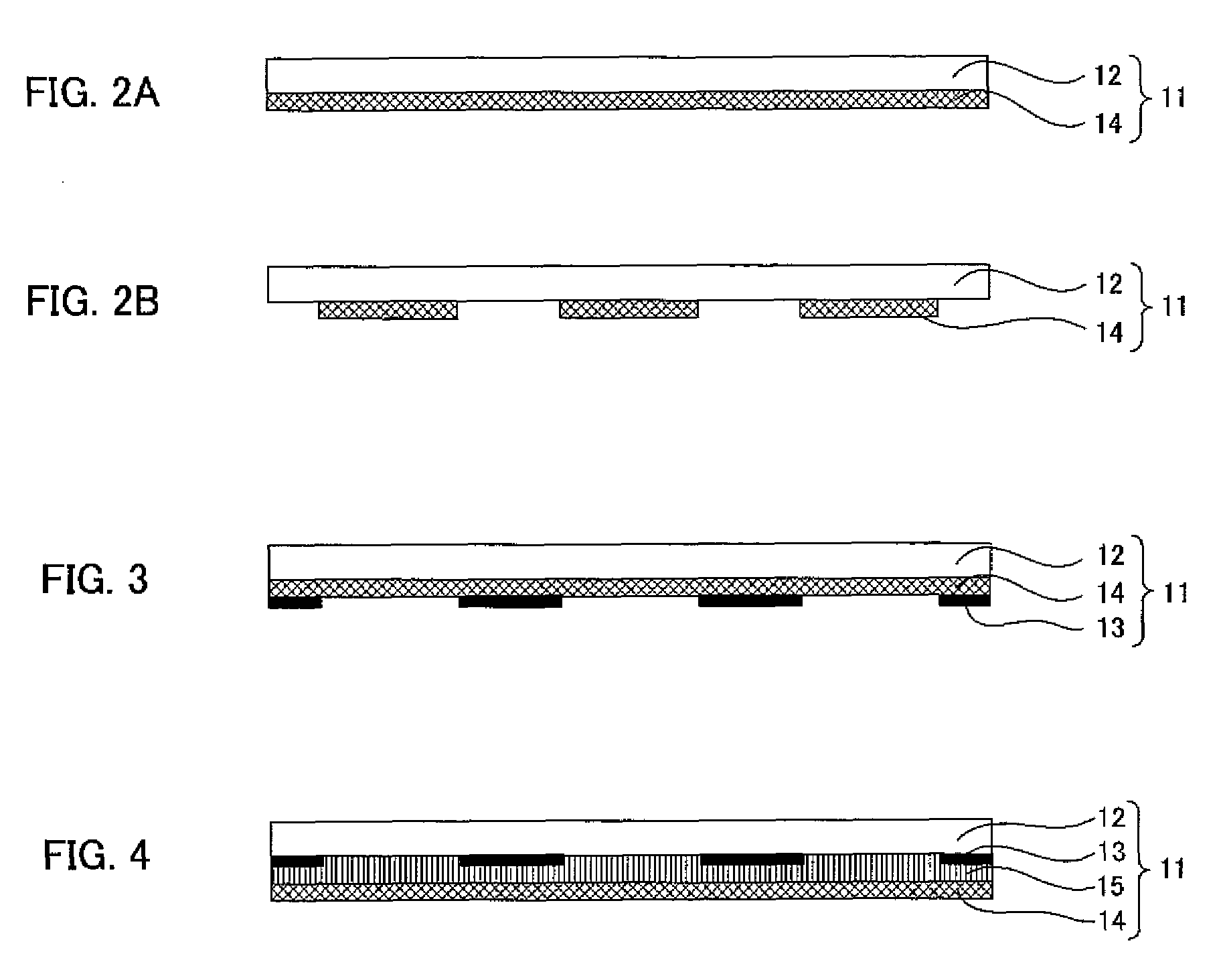
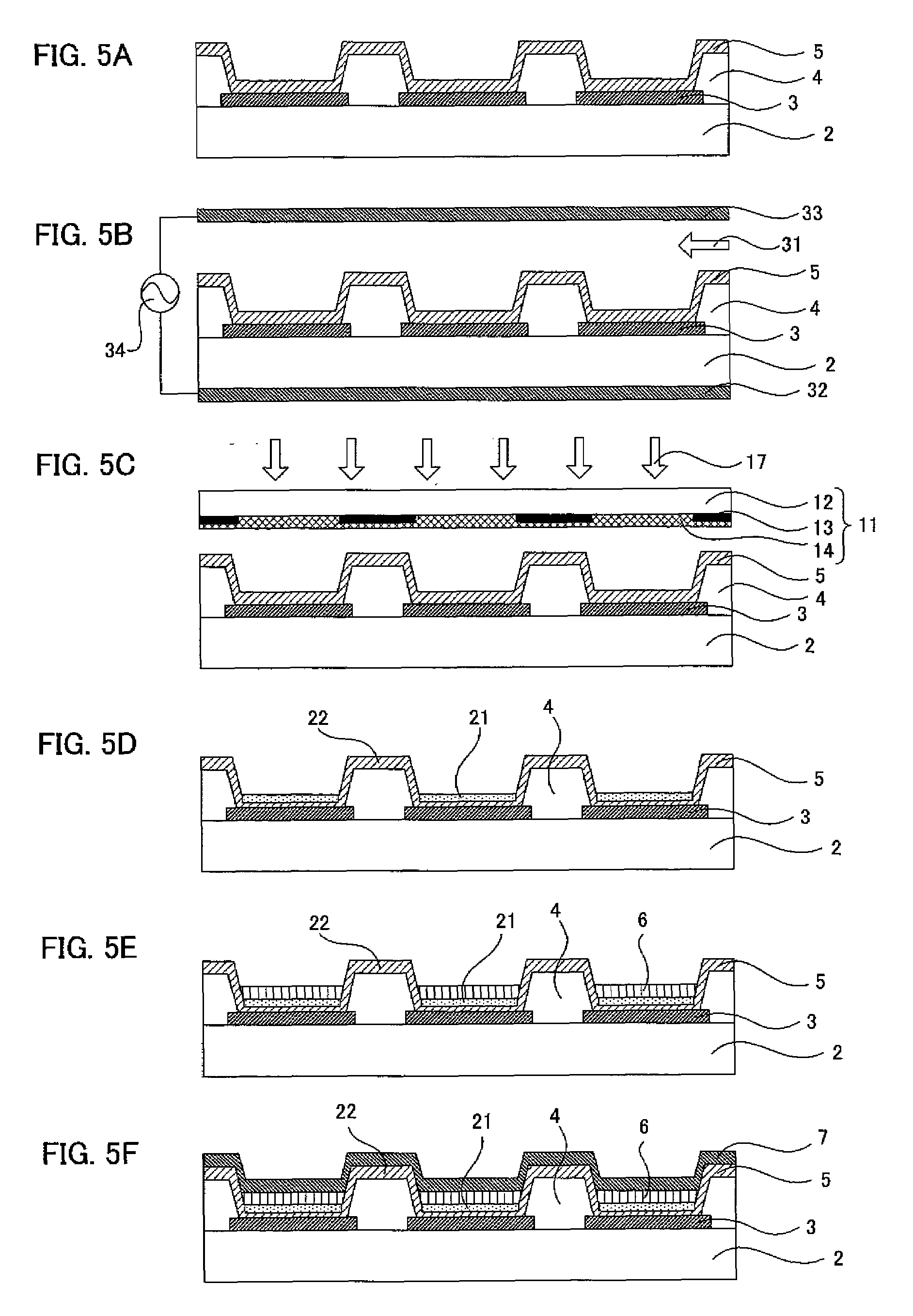
[0030]First embodiment of the manufacturing method of an organic EL element comprises: a charge injecting and transporting layer forming step of forming, on a substrate with an electrode layer formed, a charge injecting and transporting layer containing a material having a liquid repellent functional group so as to have a wettability change by an action of a photocatalyst accompanied by energy irradiation; a wettability changed pattern forming step of forming a wettability changed pattern with wettability changed on a surface of the charge injecting and transporting layer by the energy irradiation in pattern after disposing a photocatalyst processing layer substrate, in which a photocatalyst processing layer containing at least a photocatalyst is formed on a base member, with a gap capable of providing the action of the photocatalyst accompanied by the energy irradiation to the charge injecting and transporting layer; and an organic electroluminescence layer formi...

second embodiment

II. Second Embodiment

[0226]The second embodiment of a manufacturing method of an organic EL element of the present invention comprises: a charge injecting and transporting layer forming step of forming a charge injecting and transporting layer on a substrate with an electrode layer formed; a liquid repellent process step of processing the charge injecting and transporting layer surface to be liquid repellent; a wettability changed pattern forming step of forming a wettability changed pattern with wettability of the charge injecting and transporting layer surface changed by the energy irradiation in pattern after disposing the photocatalyst processing layer substrate, in which a photocatalyst processing layer containing at least a photocatalyst formed on a base member, with a gap capable of providing the action of the photocatalyst accompanied by the energy irradiation to the charge injecting and transporting layer with the liquid repellent process applied; and an organic EL layer fo...

example 1

(Formation of the Electrode Layer and the Insulation Layer)

[0292]First, a substrate comprising a glass substrate having an ITO film as the electrode layer formed in pattern of an 80 μm line width, a 20 μm space width and a 100 μm pitch was prepared.

[0293]Then, an insulation film was formed on the entire surface of the above-mentioned substrate by applying a positive type photosensitive material (OFPR-800, produced by Tokyo Ohka Kogyo Co., Ltd.) by the spin coating method so as to have a 1.5 μm film thickness. Then, exposure was carried out using a photo mask having a rectangular opening part of a 70 μm lateral width and a 70 μm longitudinal width, and development was executed with an alkaline developing solution (NMD-3, Tokyo Ohka Kogyo Co., Ltd.). Subsequently, by the heat curing process was carried out at 250° C. for 30 minutes, an insulation layer was formed in the opening part of the electrode layer.

(Formation of the Hole Injecting Layer)

[0294]A hole injecting layer forming coat...


PUM


Abstract

A main object is to provide a manufacturing method of an organic EL element having excellent light emission characteristics, and capable of facilitating the organic EL layer patterning operation and obtaining preferable wettability change. To attain the object, the present invention provides a manufacturing method of an organic EL element comprising: a charge injecting and transporting layer forming step of forming a charge injecting and transporting layer containing a material having a liquid repellent functional group so as to have the wettability change by the action of the photocatalyst accompanied by the energy irradiation on a substrate with an electrode layer formed; a wettability changed pattern forming step of forming a wettability changed pattern with the wettability of the charge injecting and transporting layer surface changed by the energy irradiation in pattern after disposing the photocatalyst processing layer substrate, in which the photocatalyst processing layer containing at least a photocatalyst is formed on a base member, with a gap capable of providing the action of the photocatalyst accompanied by the energy irradiation to the charge injecting and transporting layer; and an organic EL layer forming step of forming an organic EL layer, which includes at least a light emitting layer, on the wettability changed pattern.

Description

BACKGROUND OF THE INVENTION[0001]1. Field of the Invention[0002]The present invention relates to a manufacturing method of an EL element of patterning an organic electroluminescence (i.e., EL) layer using a layer whose wettability changes by the action of a photocatalyst accompanied by the energy irradiation.[0003]2. Description of the Related Art[0004]EL elements are for coupling a hole and an electron, injected from two electrodes facing each other, in a light emitting layer for exciting a fluorescent substance in the light emitting layer through its energy to emit a light beam of a color corresponding to the fluorescent substance, and as such gaining attention as planer display elements of a self light emission type. In particular, since organic EL displays using organic materials as light emitting materials have a high light emitting efficiency capable of realizing a high brightness light emission with an applied voltage of less than 10 V and allow the light emission in a simple...

Claims


Application Information

Patent Timeline
IPC IPC(8): B05D5/06
CPCH01L51/0004H01L51/56H01L51/5048H01L51/0005H10K71/13H10K71/135H10K50/14H10K71/00
Inventor ITO, NORIHITOIIZUMI, YASUHIRO
Owner DAI NIPPON PRINTING CO LTD
Why Eureka
Try Eureka