Semiconductor package and method of manufacturing the same

a technology of semiconductor package and semiconductor package, which is applied in the direction of bridges, bridge structure details, television systems, etc., can solve the problems of difficult to manufacture the conventional semiconductor package b>500/b>, the manufacturing process is not improved, and the size of the camera module is minimized, so as to reduce the manufacturing cost of the semiconductor packag

Inactive Publication Date: 2007-10-25
SAMSUNG ELECTRO MECHANICS CO LTD
View PDF4 Cites 81 Cited by
  • Summary
  • Abstract
  • Description
  • Claims
  • Application Information

AI Technical Summary

Benefits of technology

[0025] Therefore, the present invention has been made in view of the above problems, and it is an object of the present invention to provide a semiconductor package and a method of manufacturing the same that is capable of minimizing the size of the camera module and performing a packaging process at the wafer level step, thereby accomplishing mass production of the semiconductor package and reducing the manufacturing costs of the semiconductor package.
[0026] It is another object of the present invention to provide a semiconductor package and a method of manufacturing the same that is easily mounted through a reflow process, which is a conventional mounting process, at the step of mounting the semiconductor package on a printed circuit board (PCB), thereby improving assembly efficiency of the camera module.
[0027] It is yet another object of the present invention to provide a semiconductor package and a method of manufacturing the same that is capable of remarkably shortening a manufacturing process in chip-on-package (CSP) mode and not requiring attachment of an additional infrared (IR) filter to the camera module, thereby improving a manufacturing process of the semiconductor package and increasing productivity of the semiconductor package.

Problems solved by technology

However, the structures of the above-described conventional semiconductor packages 400 and 450 are very complicated, and therefore, it is very difficult to manufacture the conventional semiconductor packages 400 and 450.
However, the structure of this conventional semiconductor packages 500 is very complicated, and therefore, it is very difficult to manufacture the conventional semiconductor package 500.
That is, the conventional process is complicated, and therefore, improvement to the conventional process is required.

Method used


Image

  • Semiconductor package and method of manufacturing the same
  • Semiconductor package and method of manufacturing the same
  • Semiconductor package and method of manufacturing the same

Examples


Embodiment Construction

[0071] Now, preferred embodiments of the present invention will be described in detail with reference to the accompanying drawings.

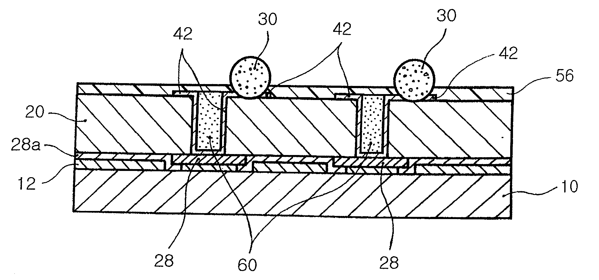
[0072] A semiconductor package 1 according to the present invention is illustrated in FIGS. 7A, 7B, and 7C. FIG. 7A is a perspective view of the semiconductor package 1 illustrating the front part of the semiconductor package 1, FIG. 7B is a perspective view of the semiconductor package 1 illustrating the rear part of the semiconductor package 1, and FIG. 7C is a longitudinal sectional view of the semiconductor package 1.

[0073] The semiconductor package 1 according to the present invention is manufactured in wafer level chip-on-package (CSP) mode. An infrared (IR) filter 10 is attached to the front surface of a wafer 20, which has an image sensor 22 formed at the center thereof. A circuit 26 is formed at the rear surface of the wafer 20, which is opposite to the image sensor 22, using a lead-redistribution technology, and solder ball-shaped bump electr...


PUM


Abstract

Disclosed herein are a semiconductor package used in digital optical instruments and a method of manufacturing the same. The semiconductor package comprises a wafer made of a silicon material and having pad electrodes formed at one side surface thereof, an IR filter attached on the pad electrodes of the wafer by means of a bonding agent, terminals electrically connected to the pad electrodes, respectively, in via holes formed at the other side surface of the wafer, which is opposite to the pad electrodes, and bump electrodes, each of which is connected to one side of each of the terminals. The present invention is capable of minimizing the size of a semiconductor package having an image sensor, which is referred to as a complementary metal oxide semiconductor (CMOS) or a charge coupled device (CCD), through the application of a wafer level package technology, thereby reducing the manufacturing costs of the semiconductor package and accomplishing production on a large scale.

Description

RELATED APPLICATIONS [0001] The present application is based on, and claims priority from, Korean Application Number 2005-8224, filed Jan. 28, 2005, the disclosure of which is incorporated by reference herein in its entirety. BACKGROUND OF THE INVENTION [0002] 1. Field of the Invention [0003] The present invention relates to a semiconductor package used in digital optical instruments and a method of manufacturing the same, and more particularly to a semiconductor package used in digital optical instruments and a method of manufacturing the same that is capable of minimizing the size of a semiconductor package having an image sensor, which is referred to as a complementary metal oxide semiconductor (CMOS) or a charge coupled device (CCD), through the application of a wafer level package technology, thereby reducing the manufacturing costs of the semiconductor package and accomplishing production on a large scale. [0004] 2. Description of the Related Art [0005] Recently, portable home...

Claims


Application Information

Patent Timeline
Patent Type & Authority Applications(United States)
IPC IPC(8): H01L21/00H01L23/12H01L27/14H04N5/335
CPCH01L23/3114H01L24/10H01L27/14618H01L2924/14H01L2924/01078H01L2924/01079H01L2924/04941H01L2924/01077H01L2924/12042H01L21/76898H01L2924/00E01D19/046G01B7/22E01D22/00
Inventor SONG, MOON KOOGKIM, DONG HWANRYU, JIN MUN
Owner SAMSUNG ELECTRO MECHANICS CO LTD
Why Eureka
Try Eureka