Nitride semiconductor device

a semiconductor and nitride technology, applied in the direction of semiconductor/solid-state device manufacturing, semiconductor devices, electrical apparatus, etc., can solve the problems of large forward gate bias, gate leakage current, flow problem, etc., and achieve the effect of wide band gap and wider band gap

Inactive Publication Date: 2007-10-25
KK TOSHIBA
View PDF4 Cites 98 Cited by
  • Summary
  • Abstract
  • Description
  • Claims
  • Application Information

AI Technical Summary

Benefits of technology

[0011] According to an aspect of the invention, there is provided a nitride semiconductor device including: a first semiconductor layer of an undoped nitride semiconductor; a second semiconductor layer of an undoped or n-type nitride semiconductor having a wider bandgap than the first semiconductor layer, the second semiconductor layer being provided on the first semiconductor layer; a p-type region selectively provided in the second semiconductor layer; a gate insulating film provided on the p-type region; a field insulating film provided on the second semiconductor layer surrounding the p-type region; a first and a second main electrodes connected to the second semiconductor layer on opposite sides of the p-type region; and a control electrode provided on the gate insulating film, at least a part of the control electrode extending on the field insulating film.
[0

Problems solved by technology

However, in this case, in order to reduce the channel resistance in a state of turn-on, a large forward gate bias is needed.
However, application of the large forward bias voltage causes a flow problem of a gate leak current.
However, if formation of a gate ins

Method used


Image

  • Nitride semiconductor device
  • Nitride semiconductor device
  • Nitride semiconductor device

Examples


Embodiment Construction

[0029] Embodiments of the invention will now be described with reference to the drawings.

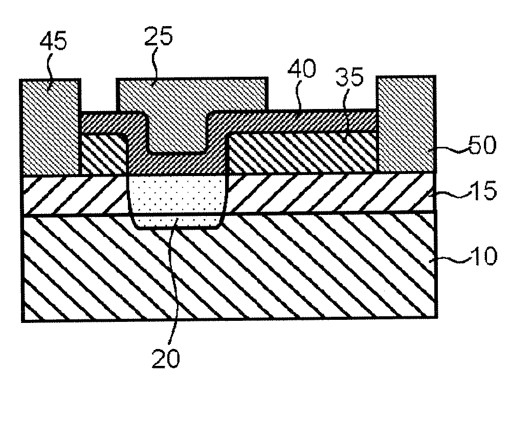
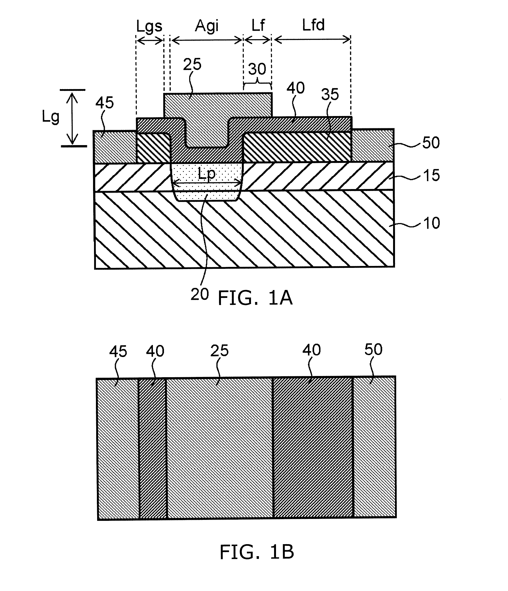
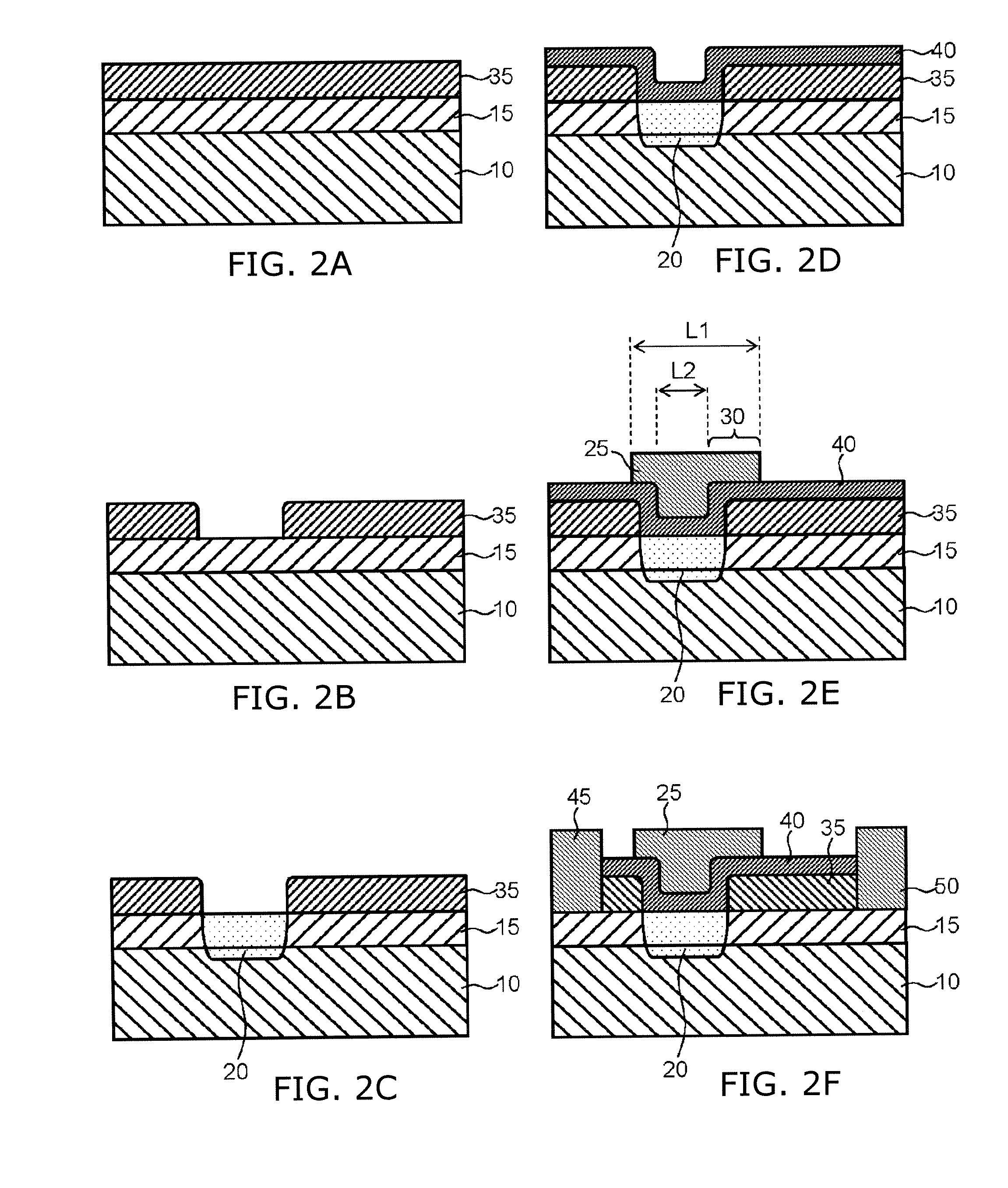
[0030]FIG. 1 shows the structure of a first example of a nitride semiconductor device according to a present embodiment, where FIG. 1A is a schematic cross section, and FIG. 1B is a schematic plan view.

[0031] In the nitride semiconductor device 5 in the present embodiment, a barrier layer 15 with a band gap broader than a channel layer 10 is provided on a major surface of the channel layer 10. Two-dimensional electron gas (2DEG) is formed in the channel layer 10 near the barrier layer 15. A sheet electron concentration of this 2DEG is, for example, on the order of 1×1013 cm−2. An field insulating film 35 having an opening and a gate insulating film 40 covering the opening provided in the field insulating film 35 are provided in this order on the major surface of the barrier layer 15. The gate insulating film 40 can be formed so as to conform to the field insulating film 35. A gate electrode 25...


PUM


Abstract

A nitride semiconductor device includes: a first semiconductor layer; a second semiconductor layer provided on the first semiconductor layer; a p-type region selectively provided in the second semiconductor layer; a gate insulating film provided on the p-type region; a field insulating film provided on the second semiconductor layer surrounding the p-type region; a first and a second main electrodes connected to the second semiconductor layer on opposite sides of the p-type region; and a control electrode provided on the gate insulating film. The first semiconductor layer is made of an undoped nitride semiconductor. The second semiconductor layer is made of an undoped or n-type nitride semiconductor having a wider bandgap than the first semiconductor layer. At least a part of the control electrode extends on the field insulating film.

Description

CROSS-REFERENCE TO RELATED APPLICATIONS [0001] This application is based upon and claims the benefit of priority from the prior Japanese Patent Application No.2006-118085, filed on Apr. 21, 2006; the entire contents of which are incorporated herein by reference. BACKGROUND OF THE INVENTION [0002] 1. Field of the Invention [0003] This invention relates to a nitride semiconductor device and more particularly to a nitride semiconductor device having a structure of a heterojunction field effect transistor. [0004] 2. Background Art [0005] Nitride semiconductor materials including gallium nitride (GaN) have a wide band gap compared with silicon (Si), thereby, exhibit a high breakdown electric field strength. Therefore, a small and high breakdown voltage device is easy to be realized. That is to say, use of a nitride semiconductor device for a power control device causes a low on-resistance and allows a low loss device to be realized. More particularly, a heterojunction field effect transi...

Claims


Application Information

Patent Timeline
IPC IPC(8): H01L31/00H01L21/8242
CPCH01L29/1066H01L29/2003H01L29/402H01L29/7787H01L29/42364H01L29/513H01L29/518H01L29/41758
Inventor SAITO, WATARU
Owner KK TOSHIBA
Why Eureka
Try Eureka