Semiconductor display device

a semiconductor display device and active matrix technology, applied in semiconductor devices, electrical appliances, instruments, etc., can solve the problems of short continuous operation time, achieve the effect of low power consumption, high power consumption of the semiconductor display device, and consume less power

Active Publication Date: 2013-05-30
SEMICON ENERGY LAB CO LTD
View PDF6 Cites 26 Cited by
  • Summary
  • Abstract
  • Description
  • Claims
  • Application Information

AI Technical Summary

Benefits of technology

[0005]Low power consumption is one of the important points in evaluating the performance of a semiconductor display device. In particular, in a portable electronic device such as a cellular phone, a semiconductor display device needs to consume less power because high power consumption of the semiconductor display device leads to a disadvantage of short continuous operating time.

Problems solved by technology

In particular, in a portable electronic device such as a cellular phone, a semiconductor display device needs to consume less power because high power consumption of the semiconductor display device leads to a disadvantage of short continuous operating time.

Method used


Image

  • Semiconductor display device
  • Semiconductor display device
  • Semiconductor display device

Examples


embodiment 1

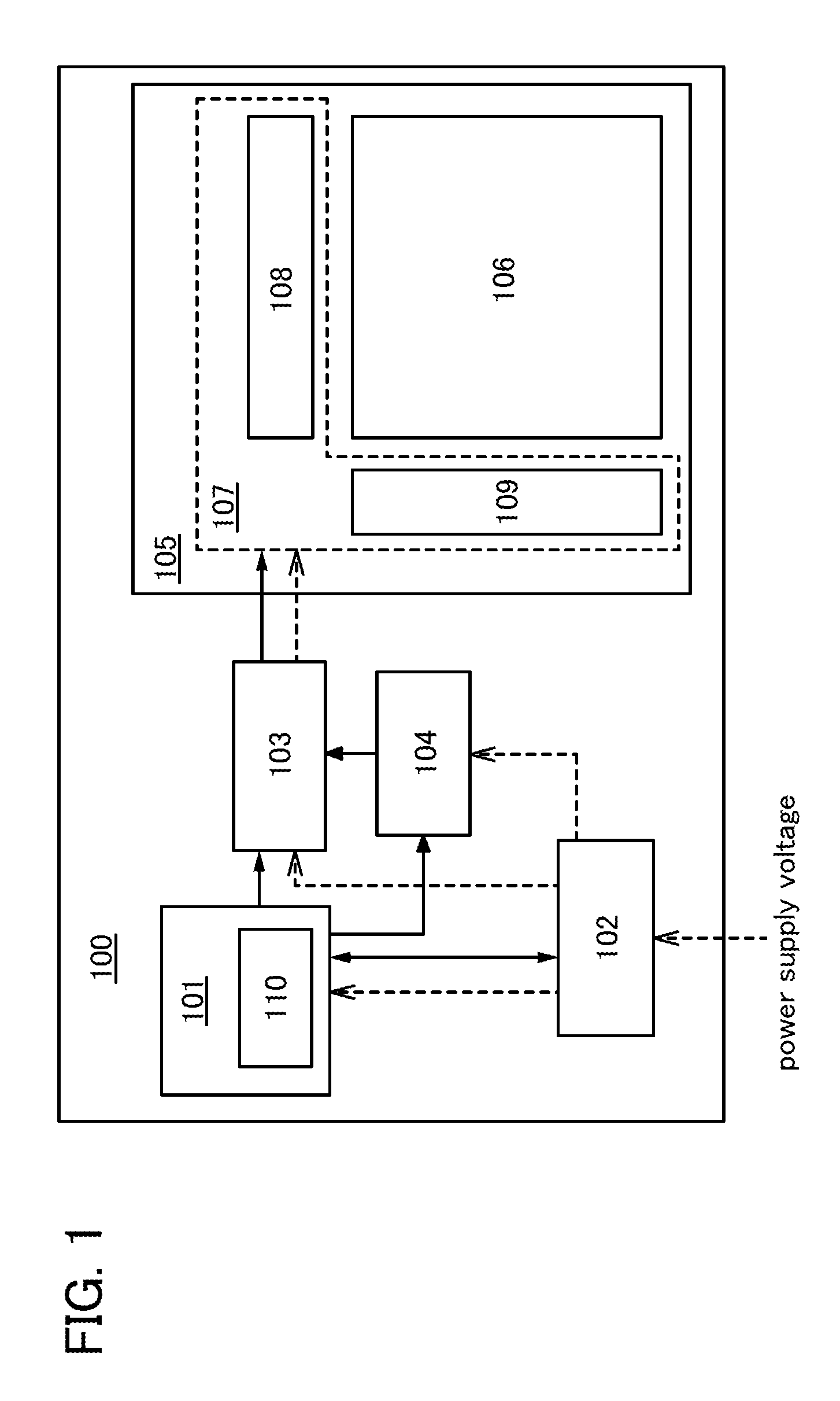
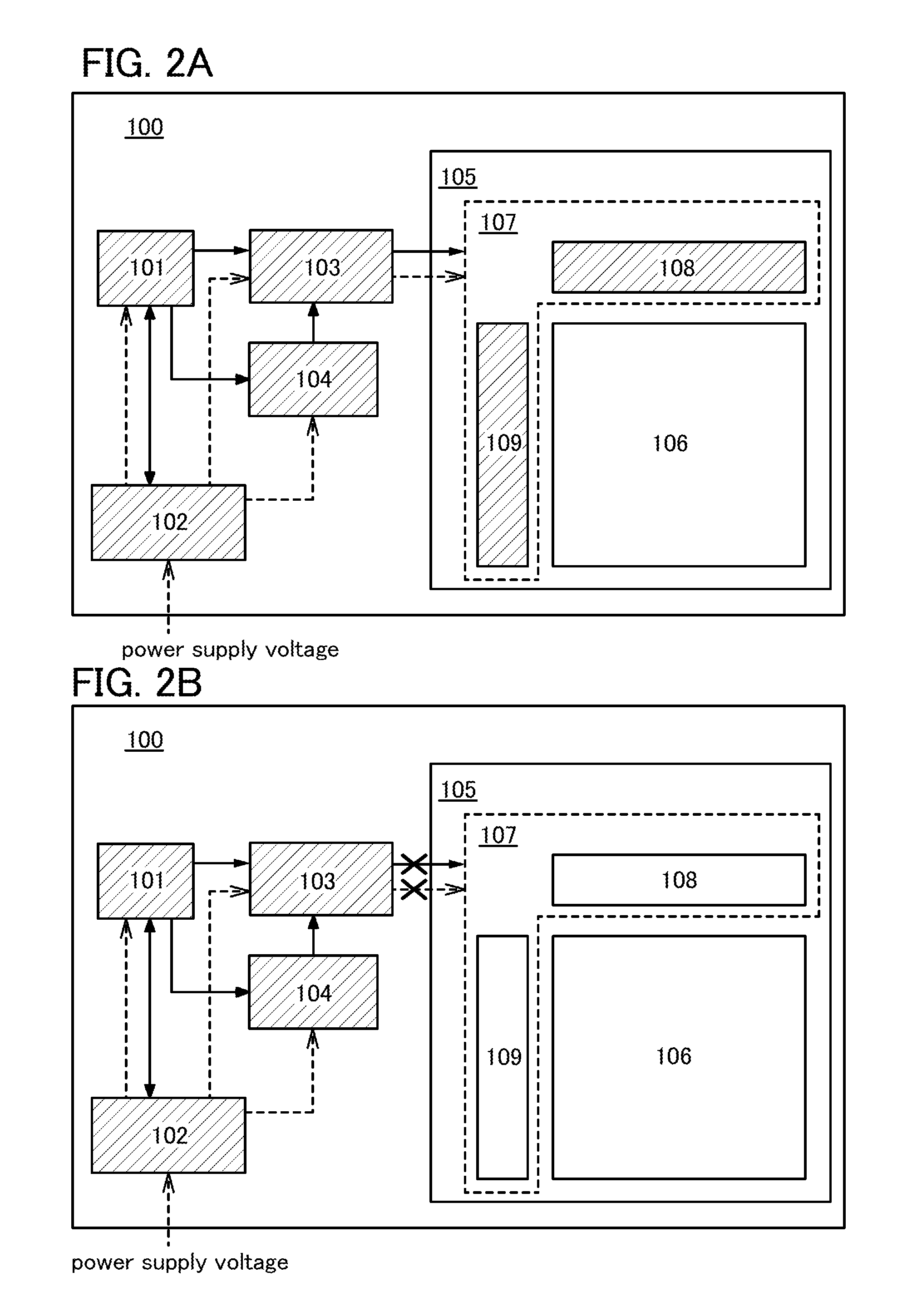
[0033]FIG. 1 illustrates a block diagram of a semiconductor display device according to one embodiment of the present invention. Note that in this specification, in a block diagram, circuits are classified by their functions and independent blocks are illustrated. However, it is difficult to classify actual circuits by their functions completely and, in some cases, one circuit has a plurality of functions.

[0034]As illustrated in FIG. 1, a semiconductor display device 100 according to one embodiment of the present invention includes a CPU 101, a power supply controller 102, a panel controller 103, an image memory 104, and a panel 105. Further, the panel 105 includes a pixel portion 106 having a display element in each pixel and a driver circuit 107 for controlling the operation of the pixel portion 106. The driver circuit 107 includes a signal line driver circuit 108, a scan line driver circuit 109, and the like.

[0035]The CPU 101 has a function of collectively controlling the operati...

embodiment 2

[0204]In this embodiment, an example of a shift register applicable to the scan line driver circuit 109 and the signal line driver circuit 108 of the semiconductor display device 100 described in the above embodiment is described.

[0205]FIGS. 11A and 11B illustrate a structure example of the shift register in this embodiment.

[0206]The shift register in FIG. 11A is formed using P sequential logic units 10 (P is a natural number of 3 or more). In FIG. 11A, the P sequential logic units 10 are illustrated as sequential logic units FF_1 to FF_P.

[0207]A start signal ST and a reset signal Res are input to each of the sequential logic units FF_1 to FF_P.

[0208]Further, a clock signal CK1, a clock signal CK2, and a clock signal CK3 are input to each of the sequential logic units FF_1 to FF_P. As the clock signal CK1, the clock signal CK2, and the clock signal CK3, for example, any three of a first clock signal (also referred to as CLK1), a second clock signal (also referred to as CLK2), a thir...

embodiment 3

[0235]In this embodiment, a specific embodiment of a CPU is described. FIG. 13 is a block diagram illustrating a structure example of a CPU.

[0236]A CPU 600 includes a controller 601, an arithmetic logic unit (ALU) 602 corresponding to an arithmetic unit, a data cache 603, an instruction cache 604, a program counter 605, an instruction register 606, a main storage device 607, and a register file 608.

[0237]The controller 601 has a function of decoding and executing an instruction input. The ALU 602 has a function of performing a variety of arithmetic processing such as four arithmetic operations and logic operations. The data cache 603 is a buffer storage device that temporarily stores frequently used data. The instruction cache 604 is a buffer storage device that temporarily stores a frequently used instruction of instructions (programs) sent to the controller 601. The program counter 605 is a register that stores an address of an instruction to be executed next. The instruction regi...


PUM


Abstract

In the case where a still image is displayed on a pixel portion having a pixel, for example, a driver circuit for controlling writing of an image signal having image data to the pixel portion stops by stopping supply of power supply voltage to the driver circuit, and writing of an image signal to the pixel portion is stopped. After the driver circuit stops, supply of power supply voltage to a panel controller for controlling the operation of the driver circuit and an image memory for storing the image data is stopped, and supply of power supply voltage to a CPU for collectively controlling the operation of the panel controller, the image memory, and a power supply controller for controlling supply of power supply voltage to a variety of circuits in a semiconductor display device is stopped.

Description

TECHNICAL FIELD[0001]The present invention relates to an active-matrix semiconductor display device including a transistor in a pixel.BACKGROUND ART[0002]In recent years, a metal oxide having semiconductor characteristics called an oxide semiconductor has attracted attention as a novel semiconductor having high mobility provided by crystalline silicon and uniform element characteristics provided by amorphous silicon. The metal oxide is used for various applications. For example, indium oxide, which is a well-known metal oxide, is used for a light-transmitting pixel electrode in a liquid crystal display device, a light-emitting device, or the like. Examples of such a metal oxide having semiconductor characteristics include tungsten oxide, tin oxide, indium oxide, and zinc oxide. Transistors each including such a metal oxide having semiconductor characteristics in a channel formation region have been known (Patent Documents 1 and 2).REFERENCE[0003]Patent Document 1: Japanese Published...

Claims


Application Information

Patent Timeline
Patent Type & Authority Applications(United States)
IPC IPC(8): H01L33/16
CPCH01L33/16H01L27/1225G02F2001/136295G09G2330/022G09G3/3648G02F1/136295H10B99/00G09G3/3614G09G3/3677G09G5/393G09G5/395G09G2300/0842G09G2310/0264G09G2330/021G09G2360/121H01L29/24H01L29/7869
Inventor NISHIJIMA, TATSUJIYONEDA, SEIICHIOHMARU, TAKUROKOYAMA, JUN
Owner SEMICON ENERGY LAB CO LTD
Why Eureka
Try Eureka