Semiconductor device and manufacturing method thereof

a technology of semiconductor devices and semiconductors, applied in semiconductor devices, resistors, diodes, etc., can solve the problems of inability to obtain a sufficiently large resistance value, difficulty in sufficiently increasing the junction area of bidirectional zener diodes, etc., and achieves a large tolerance for static electricity and sufficient static electricity.

Active Publication Date: 2007-11-01
NISSAN MOTOR CO LTD
View PDF8 Cites 24 Cited by
  • Summary
  • Abstract
  • Description
  • Claims
  • Application Information

AI Technical Summary

Benefits of technology

[0010]The present invention has been made in consideration for the problems as described above. It is an object of the present invention to provide a semiconductor device as a heterojunction field effect transistor, in which it is made possible, without bringing a large increase of manufacturing steps, to sufficiently increase the junction area of the bidirectional Zener diode of the electrostatic discharge protection element as an electrostatic protection passive element, and further to sufficiently increase the resistance value of the protection resistor for the protection from the entrance of the static electricity to the gate electrode (for protecting the gate electrode), and the tolerance for the static electricity is thereby made large. The object of the present invention is also to provide a manufacturing method of the above-described semiconductor device.
[0012]According to the semiconductor device of the present invention, the configuration is adopted, in which the electrostatic protection passive element for the heterojunction transistor is formed by overlapping the two layers of semiconductor regions with each other. Accordingly, the electrostatic protection passive element can be formed into a mode in which a sufficient tolerance for the static electricity is obtained even in such a restricted narrow region on the chip plane. For example, the junction area of the bidirectional Zener diode that composes the electrostatic protection passive element can be made sufficiently large, and accordingly, the internal resistance of the electrostatic discharge element concerned after the breakdown thereof can be made sufficiently small. Then, an effect is obtained that a semiconductor device having a large tolerance for the static electricity can be provided.

Problems solved by technology

Therefore, there has been a problem that it is difficult to sufficiently increase the junction area of the bidirectional Zener diode, to sufficiently reduce the internal resistance of the electrostatic discharge protection element after the breakdown thereof, and to thereby obtain a sufficient electrostatic tolerance of the semiconductor device.
Meanwhile, the resistance value of such an electrostatic entrance protection resistor formed of the polycrystalline silicon is also regulated only by the single layer of the polycrystalline silicon, and accordingly, there has been a problem that a sufficiently large resistance value cannot be obtained, which enables the sheet resistance of the resistor to be sufficiently larger than the sheet resistance of the gate electrode and enables the static electricity in the gate electrode to be diffused rapidly at a desired speed.

Method used


Image

  • Semiconductor device and manufacturing method thereof
  • Semiconductor device and manufacturing method thereof
  • Semiconductor device and manufacturing method thereof

Examples


first embodiment

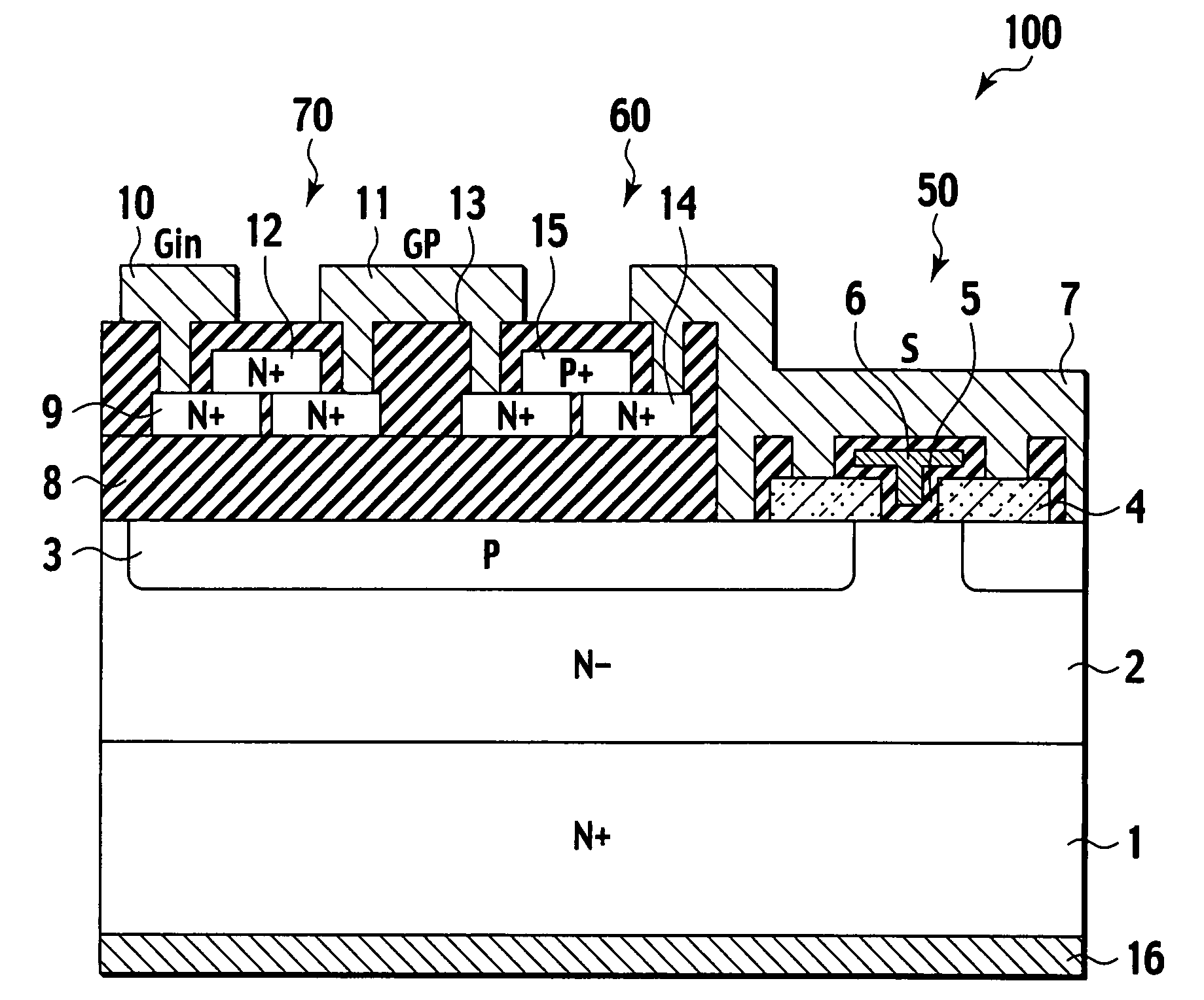
[0033]A description will be made of a configuration of a semiconductor device in a first embodiment of the present invention by using FIG. 1. FIG. 1 is a cross-sectional view schematically showing a structure of a device cross section of a field effect transistor in the first embodiment of the semiconductor device according to the present invention.

[0034]Configuration Example

[0035]In a semiconductor device 100 of FIG. 1, a right-side portion of the drawing shows a unit cell of a heterojunction field effect transistor 50. Although a plurality of the unit cells actually form the transistor by being parallelly connected, a description will be made of the transistor concerned by using this cross-sectional structure as a representative. Moreover, a left-side portion of the drawing shows a configuration of an electrostatic discharge protection element 60 and a protection resistor 70, which are formed as an electrostatic protection passive element on a field oxide film 8, that is, on a fie...

second embodiment

[0092]Next, a description will be made of a device structure of a second embodiment of the semiconductor device according to the present invention.

[0093]Configuration Example

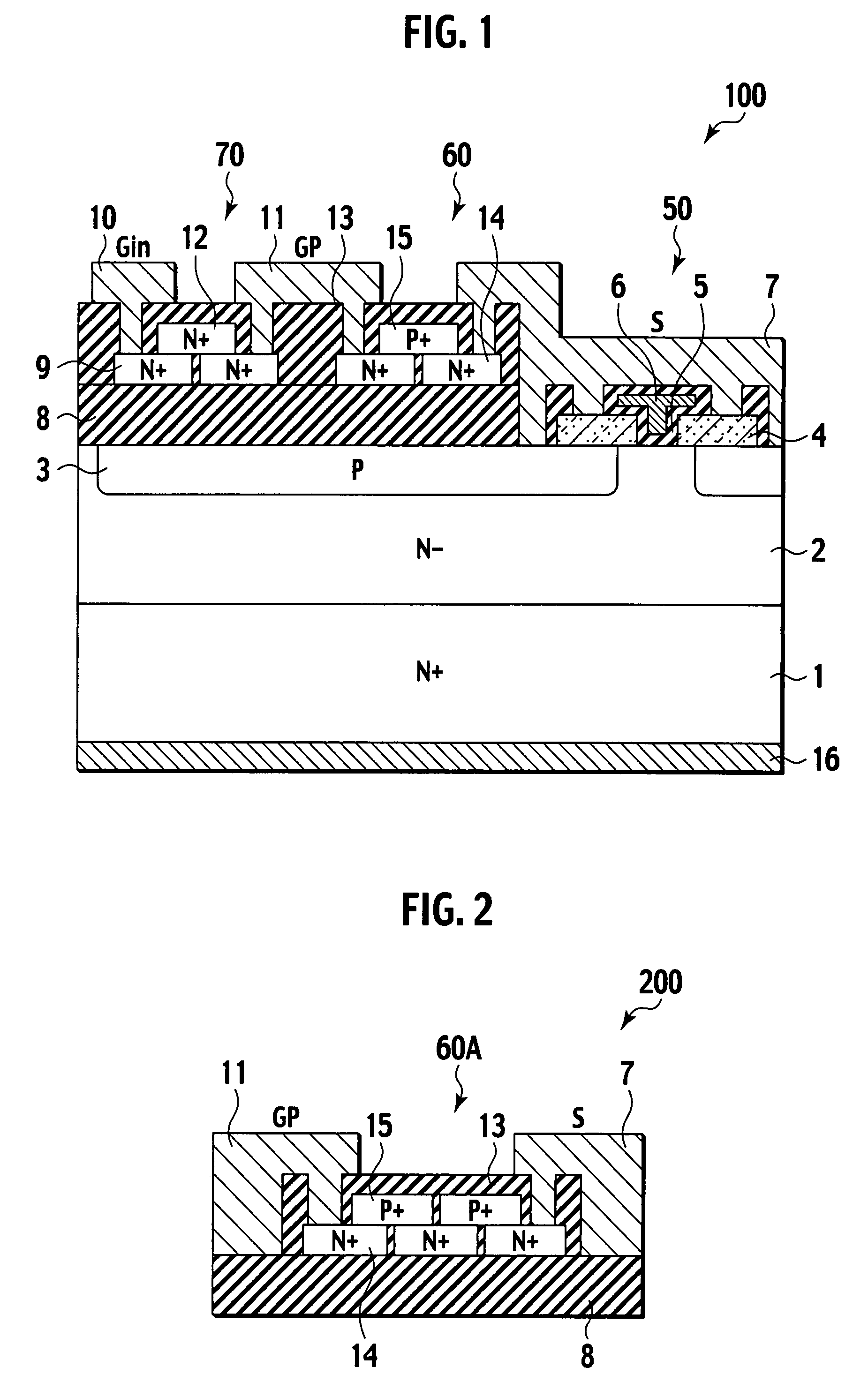
[0094]FIG. 2 is a cross-sectional view schematically showing a structure of a device cross section of a field effect transistor in the second embodiment of the semiconductor device according to the present invention. A basic entire configuration of the semiconductor device 200 of FIG. 2 is substantially similar to that of the semiconductor device 100 of FIG. 1, which is shown in the first embodiment, and a description will be made below only of portions different from those of the semiconductor device 100 of FIG. 1.

[0095]Note that the semiconductor device 200 of FIG. 2 is one in which only the region on the field oxide film 8, where an electrostatic discharge protection element 60A is present, is extracted, and the regions of the field effect transistor 50 and protection resistor 70 of FIG. 1 are similar to thos...

third embodiment

[0099]Next, a description will be made of a device structure of a third embodiment of the semiconductor device according to the present invention.

[0100]Configuration Example

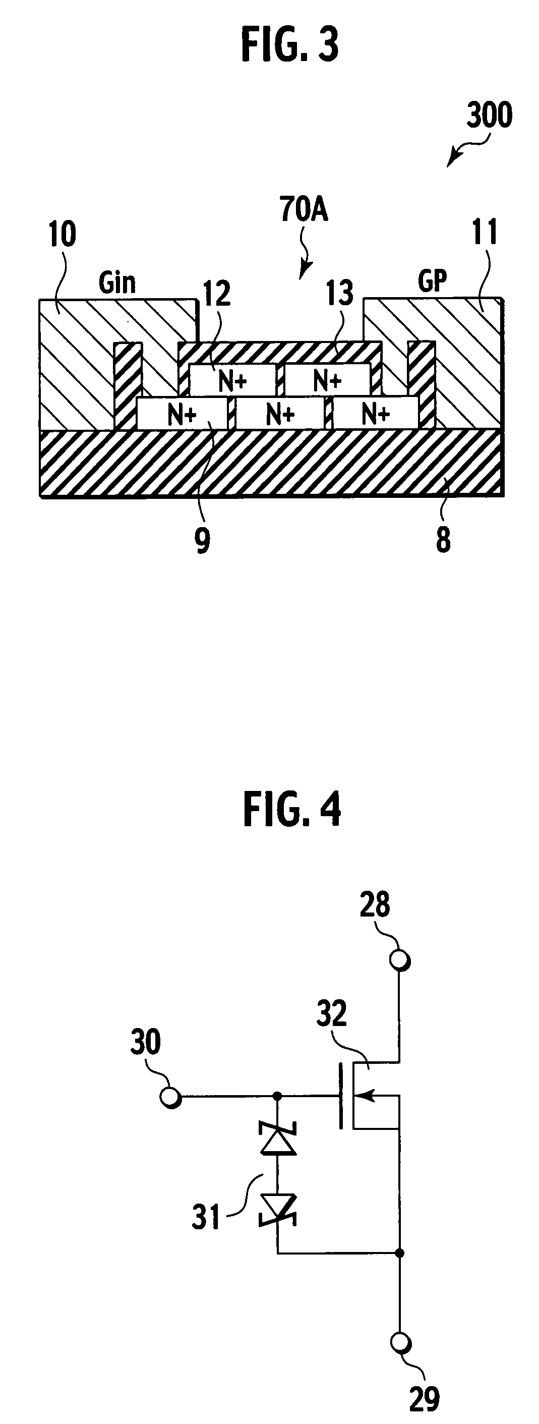
[0101]FIG. 3 is a cross-sectional view schematically showing a structure of a device cross section of a field effect transistor in the third embodiment of the semiconductor device according to the present invention. A basic entire configuration of the semiconductor device 300 of FIG. 3 is substantially similar to the semiconductor device 100 of FIG. 1, which is shown in the first embodiment, and a description will be made below only of portions different from those of the semiconductor device 100 of FIG. 1.

[0102]Note that the semiconductor device 300 of FIG. 3 is one in which only the region on the field oxide film 8, where a protection resistor 70A is present, is extracted, and the regions of the field effect transistor 50 and electrostatic discharge protection element 60 of FIG. 1 are similar to those of the se...


PUM


Abstract

An electrostatic discharge protection element and a protection resistor, which are formed on an N-drain region with a field oxide film interposed therebetween for the purpose of preventing electrical breakdown of a field effect transistor, are composed as a stacked bidirectional Zener diode of one or a plurality of N+ polycrystalline silicon regions of a first layer and a P+ polycrystalline silicon region of a second layer, and a stacked resistor of one or a plurality of N+ resistor layers of the first layer and an N+ resistor layer of the second layer, respectively. One end of the plurality of N+ polycrystalline silicon regions of the first layer is connected to an external gate electrode terminal, and the other end is connected to a source electrode. One end of the plurality of N+ resistor layers of the first layer is connected to a gate electrode, and the other end is connected to the external gate electrode terminal. Semiconductor regions of the first layer and the second layer are formed by using semiconductor films, which form a hetero semiconductor region and the gate electrode, respectively.

Description

BACKGROUND OF THE INVENTION[0001]1. Field of the Invention[0002]The present invention relates to a semiconductor device and a manufacturing method thereof.[0003]2. Description of the Related Art[0004]As a conventional technology serving as a background of the present invention, there is a semiconductor device described in Japanese Patent Laid-Open Publication No. H6-342915 “MOS Type Power Semiconductor Device Including Protection Element and Manufacturing Method Thereof” shown in Patent Document 1. The semiconductor device described in Patent Document 1 includes not only a mechanism for discharging static electricity applied to an external gate electrode terminal exposed to the outside but also a resistor having a large sheet resistance, which is for use in protecting a gate electrode from the static electricity, in a gate electrode terminal, thus making it possible to effectively prevent a breakage of a gate insulating film owing to the static electricity.[0005]Specifically, in Pat...

Claims


Application Information

Patent Timeline
Patent Type & Authority Applications(United States)
IPC IPC(8): H01L29/74H01L21/336H01L29/12H01L29/78
CPCH01L27/0255H01L28/20H01L29/1608H01L29/866H01L29/267H01L29/66068H01L29/7828H01L29/161
Inventor SHIMOIDA, YOSHIOHOSHI, MASAKATSUHAYASHI, TETSUYATANAKA, HIDEAKIYAMAGAMI, SHIGEHARU
Owner NISSAN MOTOR CO LTD
Why Eureka
Try Eureka