Redundancy-function-equipped semiconductor memory device made from ECC memory

a technology of memory device and redundancy function, which is applied in the field of semiconductor memory device having a redundancy function, can solve the problems of data access time and cycle time penalty, error correction is performed, and computation time for error correction is necessary

Inactive Publication Date: 2007-11-01
FUJITSU MICROELECTRONICS LTD
View PDF39 Cites 96 Cited by
  • Summary
  • Abstract
  • Description
  • Claims
  • Application Information

AI Technical Summary

Benefits of technology

[0021]According to one embodiment of the present invention, an ECC memory is modified such that the first data (data to be written/read) and the second data (error-correction-purpose redundant bits) are input/output in parallel, with the error correction function being set to the “off” state. With this slight design modification, the memory cells corresponding to the second data can be used for the purpose of storing normal data. In such a modified ...

Problems solved by technology

If error is detected, error correction is performed.
However, the computation time for error correction is necessary, and, also, there is a penalty in terms of data access time and cycle time as will be described below in the case of the above-described configuration in which the bit width of input/output data with respect to the memory core is set wider than the bit width of input/output data with respect to an interface with the exterior.
At the time of write operation, write data comprised of 32 bits is input from the exterior, but this write data alone is, not sufficient to generate redundant bits for the error correction purpose.
This gives rise to a problem in that the operation speed becomes slow, and also in that excessive...

Method used


Image

  • Redundancy-function-equipped semiconductor memory device made from ECC memory
  • Redundancy-function-equipped semiconductor memory device made from ECC memory
  • Redundancy-function-equipped semiconductor memory device made from ECC memory

Examples


first embodiment

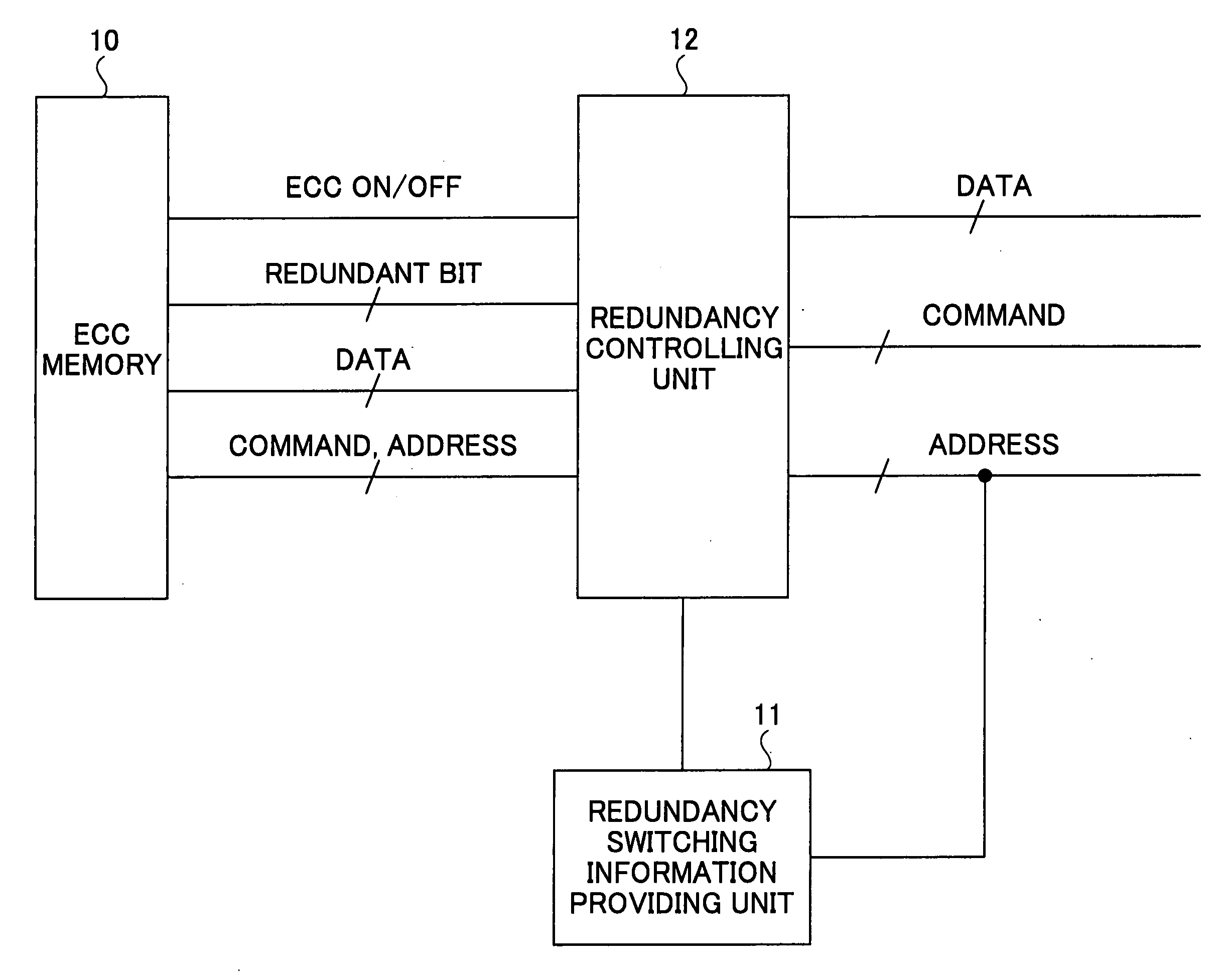
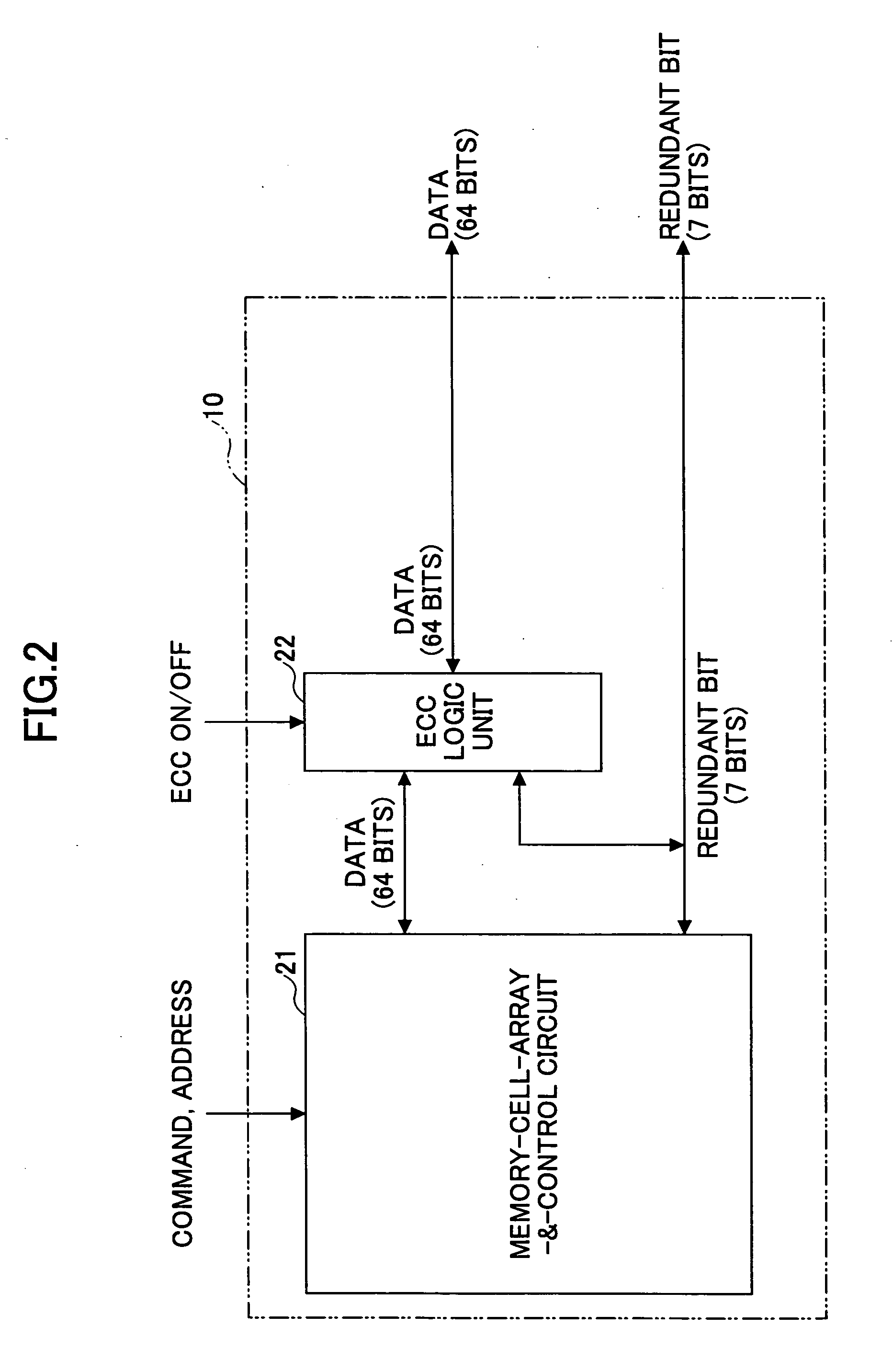
[0050]FIG. 2 is a block diagram showing the configuration of the ECC memory 10. The ECC memory 10 is identical to a conventional ECC memory, except that provision is made to input / output data of the redundancy bit portion for correcting error during the normal read / write operation. FIG. 3 is a drawing showing the configuration of a conventional ECC memory illustrated for the purpose of comparison.

[0051]The ECC memory 10 of the present invention shown in FIG. 2 includes a memory-cell-array-&-control circuit 21 and an ECC logic unit 22. The conventional ECC memory shown in FIG. 3 includes the memory-cell-array-&-control circuit 21, the ECC logic unit 22, and a selector 23. The conventional ECC memory and the ECC memory 10 of the present invention share identical configurations with respect to the memory-cell-array-&-control circuit 21 and the ECC logic unit 22. In this example, input / output data is 64 bit, and the error-correction-purpose redundant bits are 7 bits.

[0052]The convention...

second embodiment

[0074]FIG. 6 is a drawing showing the configuration of the ECC memory. In FIG. 6, the same elements as those of FIG. 2 are referred to by the same numerals, and a description thereof will be omitted.

[0075]In an ECC memory 10A shown in FIG. 6, an ECC logic unit 22A outputs an error detection signal indicative of the presence / absence of detected error and an error data position signal indicative of the bit position of an error bit contained in the read data. Other configurations are the same between the ECC memory 10 shown in FIG. 2 and the ECC memory 10A shown in FIG. 6.

[0076]In the ECC logic unit 22 of the ECC memory 10 shown in FIG. 2, as previously described, an error detection and error correction are performed with respect to read data if the ECC-on / off signal is set to the on state. An example will be examined here in which error-correction-purpose redundant bits are generated such that 71-bit data of the ECC memory 10 constitutes a Hamming code for which inter-code distance is...


PUM


Abstract

A semiconductor memory device includes a memory configured to input/output first data and second data in parallel, the first data being all or part of a predetermined number of bits, and the second data being comprised of a number of bits necessary to correct error of the predetermined number of bits, a unit configured to supply redundancy switching information in response to an address signal supplied to the memory, and a controlling unit situated between the memory and input/output nodes, having a first path that couples a given bit of the input/output nodes to a corresponding bit of the first data of the memory and a second path that couples the given bit of the input/output nodes to a predetermined bit of the second data of the memory, and configured to select and enable one of the first path and the second path in response to the redundancy switching information.

Description

CROSS-REFERENCE TO RELATED APPLICATIONS[0001]The present application is based upon and claims the benefit of priority from the prior Japanese Patent Application No. 2006-083335 filed on Mar. 24, 2006, with the Japanese Patent Office, the entire contents of which are incorporated herein by reference.BACKGROUND OF THE INVENTION[0002]1. Field of the Invention[0003]The present invention generally relates to semiconductor memory devices, and particularly relates to a semiconductor memory device having a redundancy function.[0004]2. Description of the Related Art[0005]With respect to semiconductor memory devices, the methods for fixing errors include a redundancy method that utilizes backup memory cells and a data correction method that utilizes error correcting codes (ECC).[0006]In a semiconductor memory device having the redundancy function, when a defective memory cell is in existence, such cell is replaced with a redundant memory cell serving as a backup memory cell, and an access to ...

Claims


Application Information

Patent Timeline
IPC IPC(8): G11C29/00
CPCG06F11/1008G11C29/846G11C29/42G11C29/02G11C29/00
Inventor ETO, SATOSHI
Owner FUJITSU MICROELECTRONICS LTD
Why Eureka
Try Eureka