Semiconductor laser diode with emission efficiency independent of thickness of p-type cladding layer

a technology of p-type cladding layer and emission efficiency, which is applied in the direction of semiconductor lasers, laser details, electrical devices, etc., can solve the problems of degrading the emission efficiency of the device, and achieve the reduction of the series resistance of the device, the reduction of the refractive index of the contact layer, and the suppression of the degradation of the emission efficiency

Inactive Publication Date: 2007-11-08
SUMITOMO ELECTRIC IND LTD
View PDF3 Cites 6 Cited by
  • Summary
  • Abstract
  • Description
  • Claims
  • Application Information

AI Technical Summary

Benefits of technology

[0010] Because the contact layer of the present invention contains Al and In for group III elements, the refractive index of the contact layer may be small and may suppress the light generated in the active layer to be biased in the contact layer even a thickness of the cladding layer, which is put between the active layer and the contact layer, is set to be thin. Thus, the reduction of the series resistance of the device, which may be brought by thinning the cladding layer, and the suppression of the degradation of the emission efficiency, which may be brought by the decrease of the refractive index of the contact layer, may be coped with.
[0011] The device of the present invention may provide another semiconductor layer between the cladding layer and the contact layer. This semiconductor layer may relax the band discontinuity between the cladding layer and the contact layer. Therefore, the series resistance of the device may be further decreased.

Problems solved by technology

Thinning the p-type cladding layer, which reduces the series resistance of the device, degrades the emission efficiency of the device.

Method used


Image

  • Semiconductor laser diode with emission efficiency independent of thickness of p-type cladding layer
  • Semiconductor laser diode with emission efficiency independent of thickness of p-type cladding layer
  • Semiconductor laser diode with emission efficiency independent of thickness of p-type cladding layer

Examples


Embodiment Construction

[0018] Next, preferred embodiments of the present invention will be described as referring to accompanying drawings. In the description of drawings and the specification, the same numerals or symbols will refer to the same elements without overlapping explanations.

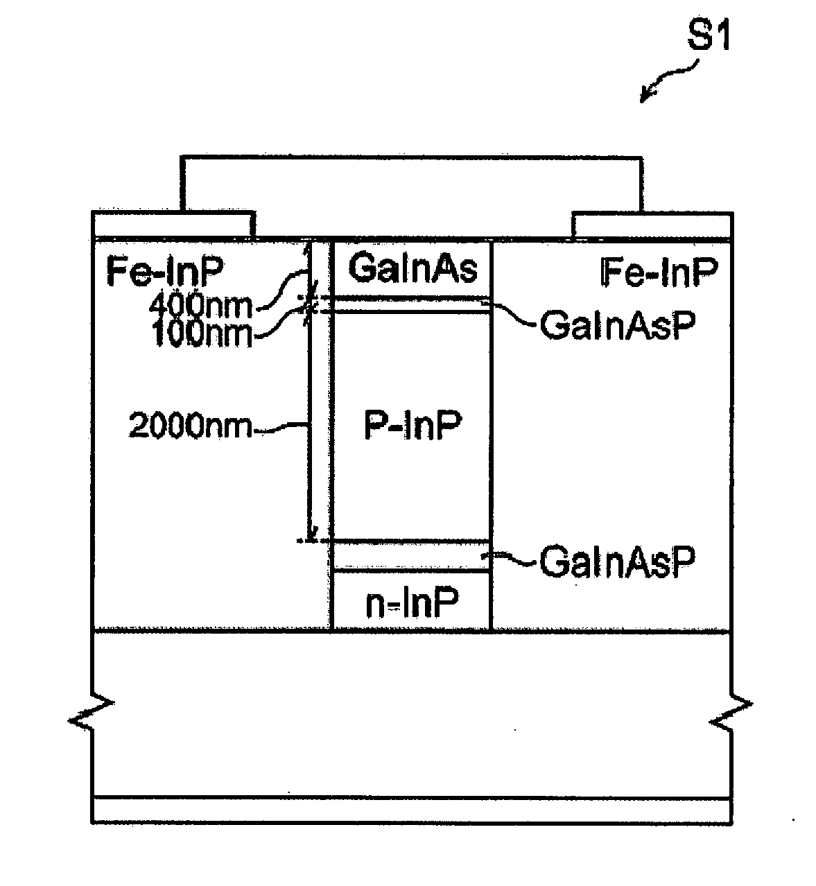
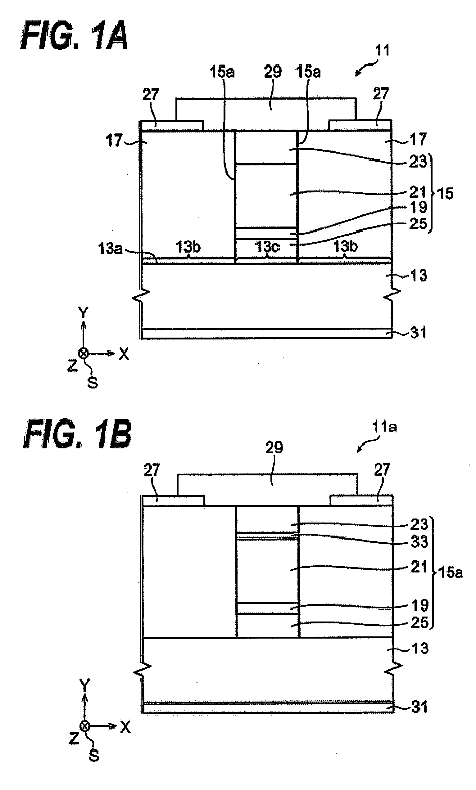
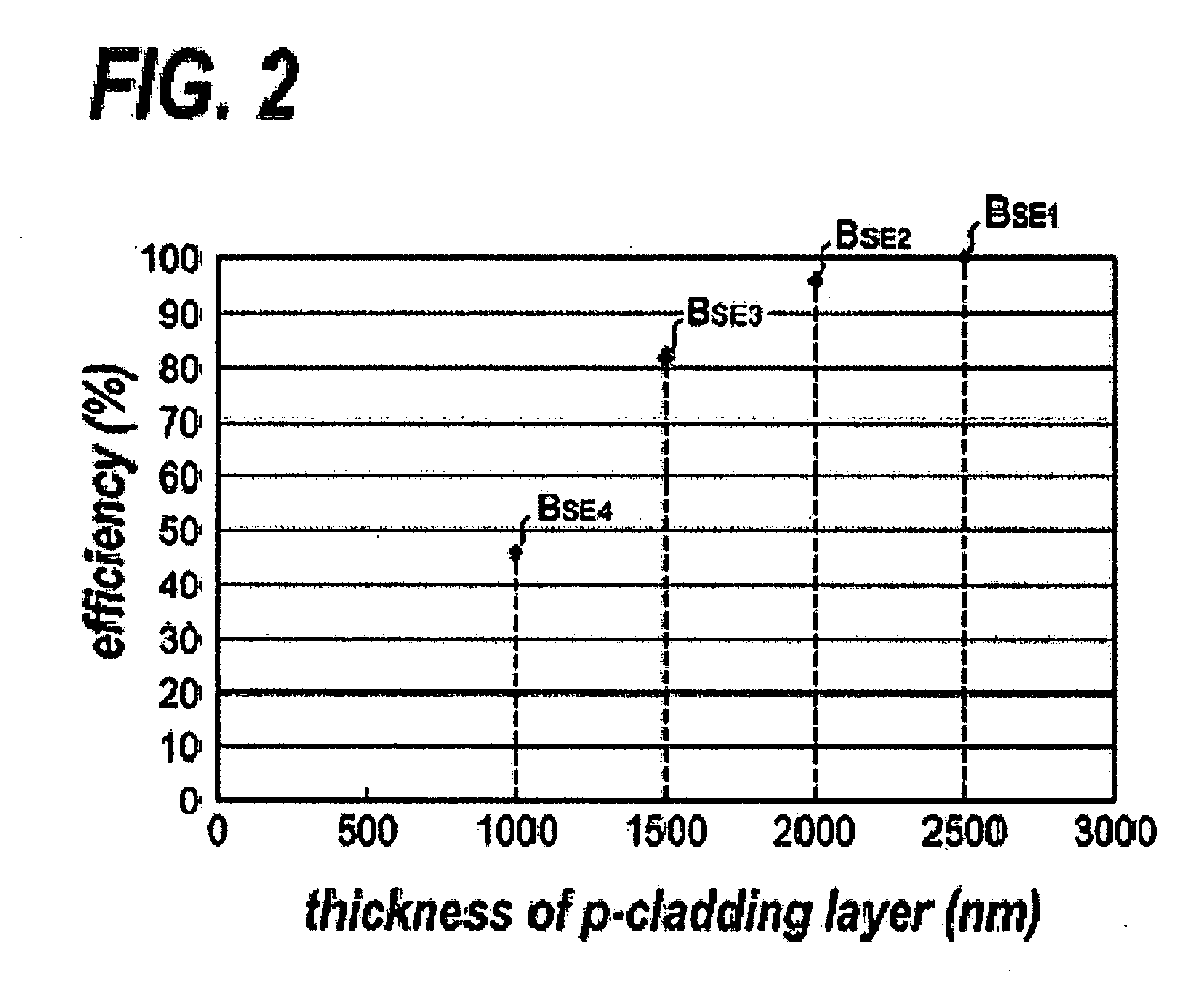
[0019]FIG. 1A is a cross section of a semiconductor optical device 11 according to an embodiment of the invention. The description below concentrates on a semiconductor laser diode as one of the semiconductor light-emitting device. The laser diode 11 includes a semiconductor substrate 13 with a first conduction type, a mesa structure 15 and regions 17 for burying the mesa. The substrate 13 is made of group III-V compound semiconductor material. The mesa 15 and the regions 17 are arranged on the substrate 13. The mesa 15 includes an active layer 19, an upper cladding layer 19 with a second conduction type and a contact layer 23 with the second conduction type. The mesa 15 may include a lower cladding layer 25 with the firs...


PUM


Abstract

A semiconductor laser diode (LD) has been disclosed, where the emission efficiency is independent on a thickness of the p-type cladding layer. The LD provides a first semiconductor region made of group III-V compound semiconductor material, a mesa region and a burying region. The burying region, disposed on the first region, buries the mesa region. The mesa region includes an active layer, a cladding layer with a first conduction type, another cladding layer with second conduction type and a contact layer with the second conduction type. The LD of the invention in the contact layer thereof contains aluminum (Al) and indium (In) for group III element, while, arsenic (As) for group V element.

Description

BACKGROUND OF THE INVENTION [0001] 1. Field of the Invention [0002] The present invention relates to a semiconductor optical device, in particular, the invention relates to a semiconductor light-emitting device. [0003] 2. Related Background Art [0004] A Japanese Patent Application published as JP-H05-082891A has disclosed a semiconductor laser diode (hereinafter denoted as LD) with a mesa structure that includes an n-type InGaAsP optical guiding layer, an un-doped InGaAsP active layer, a p-type InP cladding layer and a p-type InGaAsP contact layer. This LD further provides a semi-insulating iron-doped InP burying layer so as to bury the mesa structure in both sides thereof the structure to block the current flowing the burying layer, accordingly, to concentrate the current flowing in the mesa structure. Moreover, the LD provides another semi-insulating layer made of InGaAsP with the band gap energy smaller than that of InP, which is a material of the semiconductor substrate, so as t...

Claims


Application Information

Patent Timeline
Patent Type & Authority Applications(United States)
IPC IPC(8): H01S5/00
CPCB82Y20/00H01S5/0421H01S5/34373H01S5/2275H01S5/3211H01S5/2224
Inventor KAWAHARA, TAKAHIKOFURUKAWA, MASATO
Owner SUMITOMO ELECTRIC IND LTD
Why Eureka
Try Eureka