Optically-enabled integrated circuit package

a technology of integrated circuits and integrated circuits, applied in the field of integrated circuit (ic) packages, can solve the problems of not addressing the modularity and industry standard form-factor of semiconductors, not efficient use of space, and ever more challenging set of criteria, so as to reduce the rate at which electrical power is consumed by the microchip, reduce the signal conditioning, and increase the data rate

Active Publication Date: 2007-11-08
REFLEX PHOTONIQUE REFLEX PHOTONICS
View PDF7 Cites 67 Cited by
  • Summary
  • Abstract
  • Description
  • Claims
  • Application Information

AI Technical Summary

Benefits of technology

[0015] To address the issues of modularity and form-factor, we propose to leverage industry standard integrated circuit (IC) package form-factors such as pin-grid array (PGA) and ball-grid array (BGA) packages and augment them with planar, modular, optical sub-assemblies. This will form a hybrid optical IC package that contains both the standard electrical connections of typical IC packages as well as one or more optical ports on the sides of the package to allow optical signals to propagate to within millimeters of the microchip. These new “optically enabled” packages will continue to be assembled using standard assembly techniques such as chip-attach, wirebonding, flip-chipping, glob-top encapsulation, solder balling, and solder re-flowing so as not to disrupt the well established industry IC packaging production lines. In addition to this, the microchip designers and manufacturers will not have to modify their architectures or physical layouts since the optical conversion will occur away from the microchip. However, since the optical conversion occurs only millimeters from the microchip very high data rates can still be achieved without an exponential increase in power as in the all-electrical signaling case. Furthermore, because of the fidelity of optical signals and their immunity to crosstalk and electromagnetic effects, the rate at which electrical power is consumed by the microchip is reduced relative to the all-electrical signaling case. The reason is that an optical signal requires far less signal conditioning and signal correction (fewer transistors overall) than equivalent electrical-only signaling methods above 1-Gb / s. This allows much lower cost per gigabit per second per watt.
[0016] Some aspects of this disclosure are as follows: 1) optical alignment issues for the IC package assembly and printed circuit board (PCB) assembly are eliminated since the optical sub-assemblies have been pre-aligned optically and can be simply “dropped” into place and connected to the microchip via electrical interconnections such as wirebonds, 2) The optical sub-assembly has a standard electrical interface for the microchip in the IC package and a standard optical interface for external optical fiber cabling, 3) The chip designers and chip manufacturers do not have to alter their architectures or fabrication methods, 4) very dense and very high speed data rates can be offered directly to and from the microchip since the optical conversion takes place only a few millimeters from the microchip, 5) the typical high speed copper traces to and from the package are not necessarily required simplifying the motherboard design and eliminating extra components such as optical transceivers for the design, and 6) the rate at which electrical power is consumed is reduced for ever faster input and output signals to and from the IC package.
[0018] In an embodiment, the concept is to provide simple features surrounding the optical ports of the hybrid optically enabled IC package as well as simple attachment clips to provide mating forces between the MT optical ferrule and the optical ports on the sides of a hybrid optical IC package. This must be accomplished with a minimum amount of physical intrusiveness with respect to both the IC package and the surrounding printed circuit board (PCB). Both the PCB designer and the PCB assembler wish to minimize the size of any optical connections on the physical layout of the PCB—reserving board area on the PCB for parts that are not electrical and would never directly connect to the PCB is not an efficient use of space. It is desirable that the entire optical assembly be only slightly larger than the optical MT ferrule itself and not require any significant re-positioning of the other components on the PCB—such as heat sinks, fans, sockets, or adapters.

Problems solved by technology

Typical industry standard IC packages such as the ball grid array (BGA) package have been able to keep pace with the data rate and pin-out demands from leading edge microchip designers but are steadily facing an ever more challenging set of criteria for density and data rates in the face of growing power consumption concerns.
However, none of these technologies have properly addressed the issues of modularity and industry standard form-factor for the semiconductor market.
Both the PCB designer and the PCB assembler wish to minimize the size of any optical connections on the physical layout of the PCB—reserving board area on the PCB for parts that are not electrical and would never directly connect to the PCB is not an efficient use of space.

Method used


Image

  • Optically-enabled integrated circuit package
  • Optically-enabled integrated circuit package
  • Optically-enabled integrated circuit package

Examples


Embodiment Construction

[0065] In the following description of the embodiments, references to the accompanying drawings are by way of illustration of an example by which the invention may be practiced. It will be understood that other embodiments may be made without departing from the scope of the invention(s) disclosed.

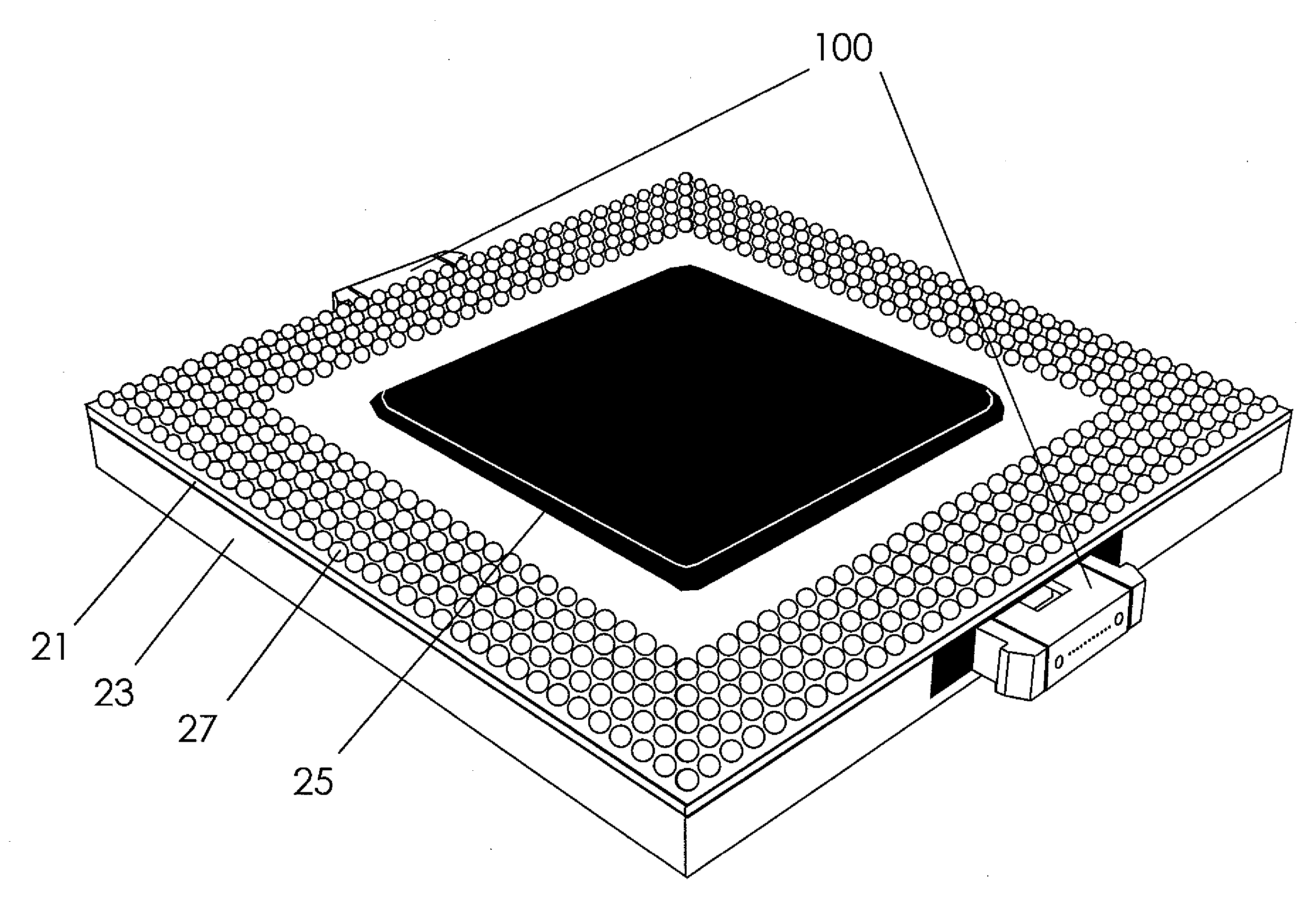
[0066] In one embodiment of the present invention, a modified cavity-down ball grid array (BGA) integrated circuit (IC) package is proposed that incorporates mechanical clearances for a modular optical sub-assembly. The optical sub-assembly (OSA) is a modular, low-profile, low-cost component with a standard electrical interface and a standard optical interface and is placed within the IC package between a user defined microchip and the side-face of the IC package. The standard optical interface on the side of the IC package also includes a means to clip or mate (and unmate) an optical patch cable directly to the side of the package. The finished optically enabled BGA IC package can then be...


PUM


Abstract

An optically-enabled integrated circuit (IC) package for connecting an electrical circuit board to an optical fiber is presented. The IC package comprises an OSA having a laser which is pre-aligned with the optical fiber. The OSA further comprises a standard electrical interface for the connection to the microchip and a standard optical interface for the connection to the optical fiber. A set of mechanical concepts for connecting optical connectors and cables to integrated circuit packages is also presented and can be applied for any type of optical connector such as single optical fiber ferrules, MT-RJ type optical ferrules and 2-D MT-type optical ferrules.

Description

CROSS-REFERENCE TO RELATED APPLICATIONS [0001] The present application claims priority under 35 U.S.C. §119(e) of U.S. provisional patent application No. 60 / 797,747 filed May 5, 2006 entitled OPTICALLY ENABLED INTEGRATED CIRCUIT PACKAGE by Rolston et al., U.S. provisional patent application No. 60 / 798,301 filed May 8, 2006 entitled OPTICALLY ENABLED INTEGRATED CIRCUIT PACKAGE by Rolston et al., and U.S. provisional patent application No. 60 / 894,998 filed Mar. 15, 2007 entitled OPTICAL MATING FOR OPTICALLY-ENABLED IC PACKAGES by Rolston et al. The specifications of the foregoing provisional applications are hereby incorporated by reference.FIELD OF THE ART [0002] The present disclosure relates to the field of integrated circuit (IC) packages for ultra-high speed optical interconnection applications. BACKGROUND OF THE ART [0003] The efficient transmission of data between the integrated circuit (or microchip) and the external world has been the focus of intense engineering for IC packa...

Claims


Application Information

Patent Timeline
Patent Type & Authority Applications(United States)
IPC IPC(8): G02B6/36
CPCG02B6/3897G02B6/4232G02B6/4292H01L2924/0002G02B6/43H01L2924/00
Inventor ROLSTON, DAVID ROBERT CAMERONMAINARDI, RICHARDFU, SHAO-WEI
Owner REFLEX PHOTONIQUE REFLEX PHOTONICS
Why Eureka
Try Eureka