
Method for Improving Efficiency of a Manufacturing Process Such as a Semiconductor Fab Process

a manufacturing process and semiconductor technology, applied in the field of semiconductor fab, can solve the problems of limiting the application of integrated metrology, costing and difficult to integrate metrology tools into production equipment, and limiting the calibration of the integrated metrology itsel

Inactive Publication Date: 2007-11-08
PDF SOLUTIONS SA
View PDF19 Cites 15 Cited by
  • Summary
  • Abstract
  • Description
  • Claims
  • Application Information

AI Technical Summary

Benefits of technology

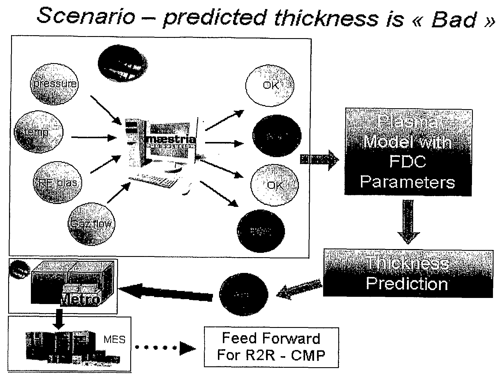
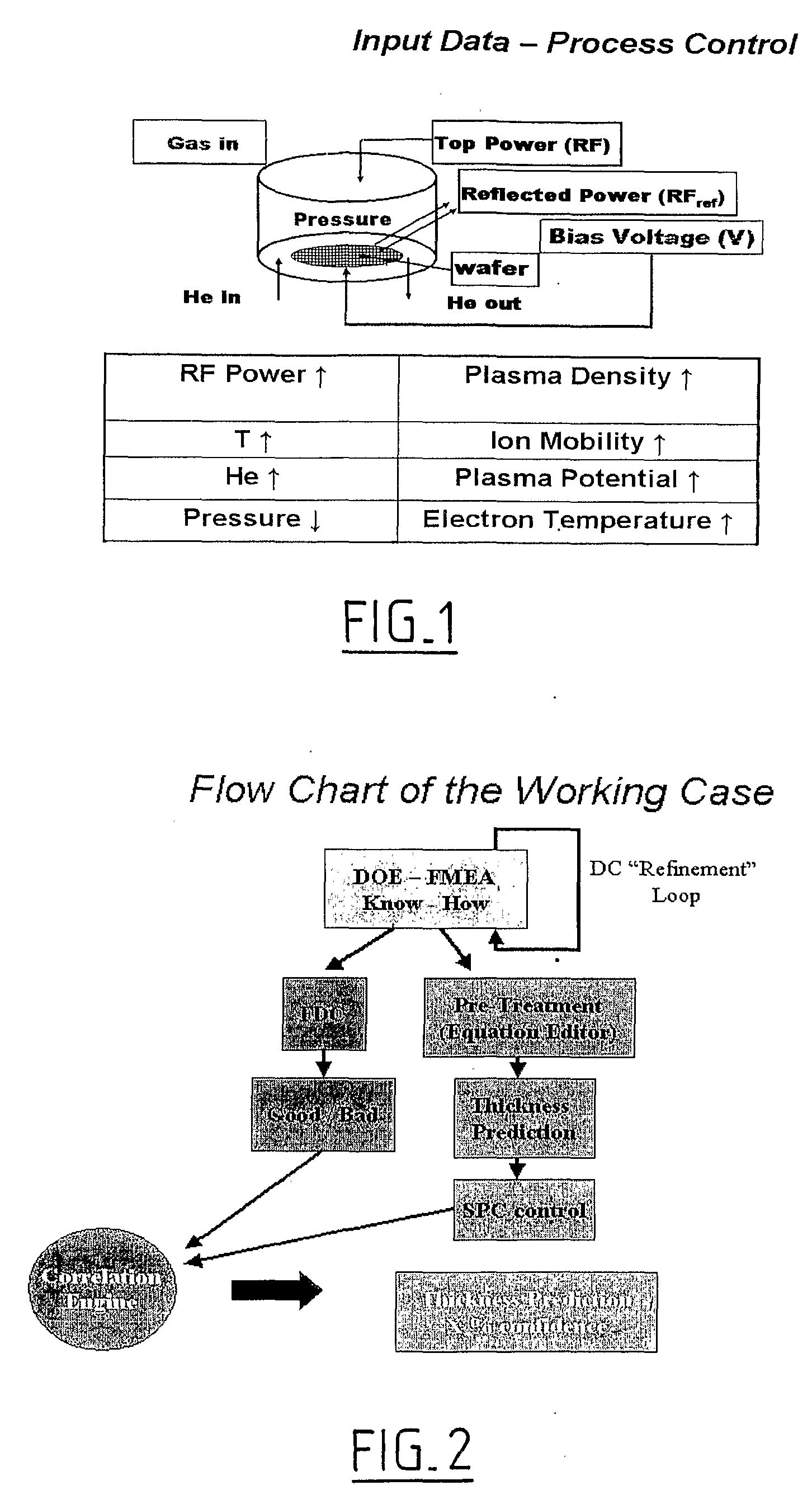
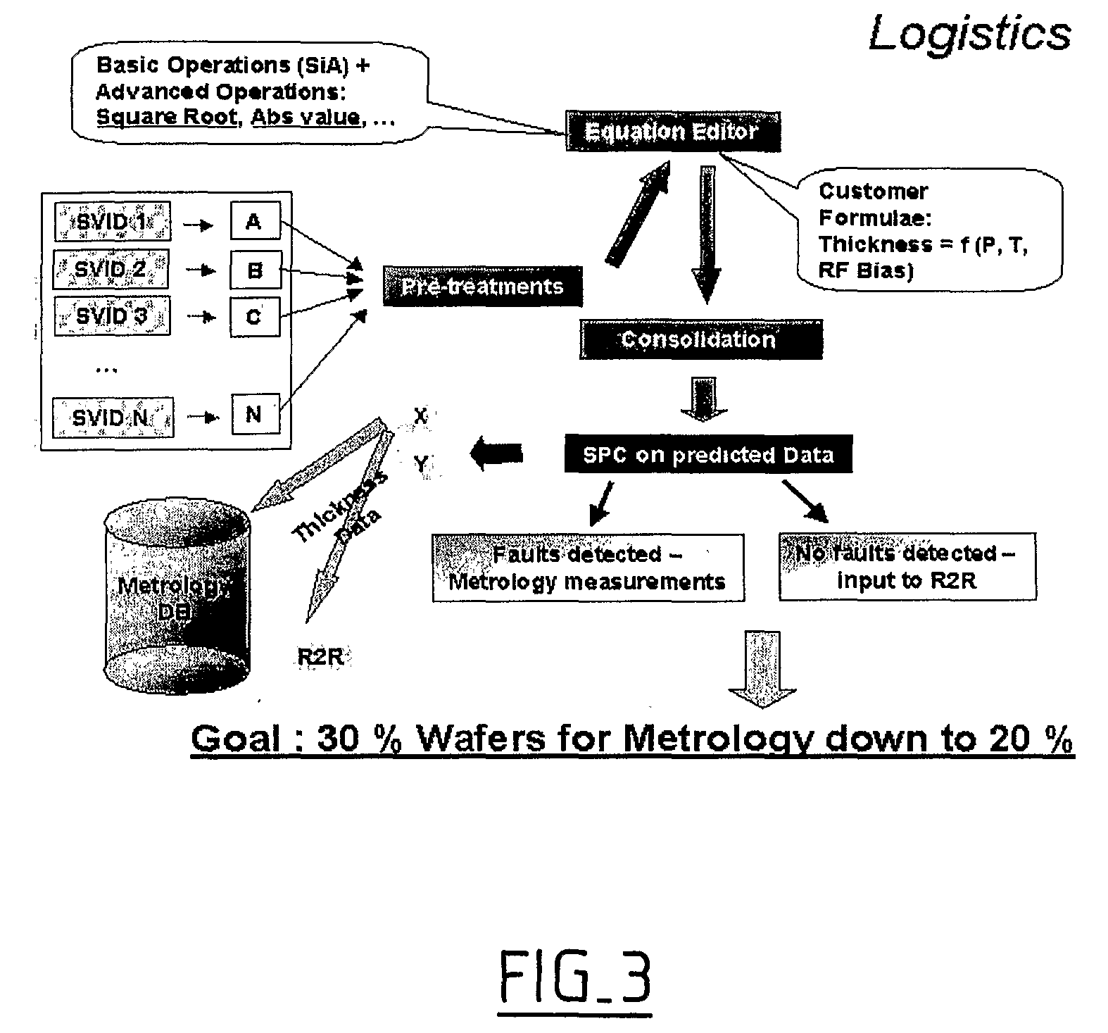
[0006] The underlying idea of the present invention is that, by applying mathematical analysis to standard, readily available FDC “input” parameters, it is possible for certain steps of a fab process to predict a quality classification of the products as output for these process steps.
[0021] According to a second aspect, the present invention provides a method for improving the efficiency of a given product manufacturing process such as CMP process based on the information retrieved from the previous processing step (plasma deposition) through FDC system and corresponding correlation algorithm. The given step of the process has a quality result which can be actually measured on each product or group of products.

Problems solved by technology

However, integration of Metrology tools into production equipment remains costly and difficult task as well as the time required for calibration of the integrated metrology itself still limits its application.

Method used


Image

  • Method for Improving Efficiency of a Manufacturing Process Such as a Semiconductor Fab Process
  • Method for Improving Efficiency of a Manufacturing Process Such as a Semiconductor Fab Process
  • Method for Improving Efficiency of a Manufacturing Process Such as a Semiconductor Fab Process

Examples


example

[0106] The above-described method has been applied to the real processing of Fluorine-doped Silicate Glass (FSG) deposition in HDP-CVD as the part of Pre-Metal layer deposition sequence. 81 wafers have been inspected by FDC and thickness prediction was performed and then matched with in-line metrology for 13 of them. The target thickness for the resulting FSG layer was 450 nm. Thickness prediction for each of the 13 wafers confronted to their in-line metrology in order to calibrate prediction algorithm.

[0107]FIG. 8 represents the results of FDC analysis on the plasma-influent parameter values for each wafer by applying Hotelling T2 statistics with detection of “above the statistical limit” T2 values. It is reminded here that Hotelling T2 is a statistical measure of the multivariate distance for each observation from the center of the data set.

[0108] A “Black” Alarm Index (i.e., important anomalies with a multivariate deviation of more than 6 sigmas from process “normality”) was co...


PUM


Abstract

The present invention provides a method for improving the efficiency of a product manufacturing process such as a semiconductor fab process, wherein a given step of the process has a quality result which can be actually measured on each product or group of products, and wherein the process comprises a subsequent, adjustable step, the method comprising:—providing a correlation model of the behavior of said given step as a function of available parameters;—for each product or group of products at the output of said manufacturing step, computing a predicted quality result based on said correlation model as a function of the actual values of the parameters during the manufacturing step, and—providing the quality result to a control system for adjusting said subsequent step.

Description

[0001] The present invention relates in general to quality monitoring in a manufacturing plant environment, and more specifically to a method of quality monitoring intended to conduct manufacturing processes in a more effective way, in particular in the environment of a semiconductor fab. BACKGROUND OF THE INVENTION [0002] In a modern semiconductor fab handling 200 mm or 300 mm semiconductor wafers, cost reduction is one of the most important factors to achieve competitiveness. For this purpose, metrology tools, Fault Detection and Classification (FDC) tools, Run-to-Run (R2R) tools and Yield Analysis tools have been introduced to make processing more efficient. [0003] More particularly, while FDC controls the process, helps to reduce scrap and number of test wafers, metrology controls the process performance by analyzing process “output” critical parameters such as deposited thickness, etch depth & rate, CD, etc. [0004] In the permanent search for maximized efficiency, it is clear t...

Claims


Application Information

Patent Timeline
IPC IPC(8): G05B19/418
CPCG05B19/41875G05B2219/32194G05B2219/32187Y02P90/02
Inventor ZAGREBNOV, MAXIM
Owner PDF SOLUTIONS SA
Learn More