Active Matrix Substrate and Display Unit Provided with It
Active Publication Date: 2007-11-22
MERCK PATENT GMBH
View PDF17 Cites 18 Cited by
Summary
Abstract
Description
Claims
Application Information
AI Technical Summary
This helps you quickly interpret patents by identifying the three key elements:
Problems solved by technology
Method used
Benefits of technology
Benefits of technology
[0010] The present invention has been made in view of the above problems, and an objective thereof is to provide: an active matrix substrate which can reduce the capacitance formed at each intersection between a scanning line and a signal line, without causing an increase in the wiring resistance or a degradation of the driving ability of switching elements; and a display device including the same.
[0046] In an active matrix substrate according to the present invention, an insulating film covering scanning lines is a multilayer insulating film including a first insulating layer and a second insulating layer, the first insulating layer being formed of an insulating material containing an organic component. Therefore, the capacitance which is formed at each intersection between a scanning line and a signal line can be reduced.
[0047] According to a first aspect of the present invention, the multilayer insulating film has a low-stack region in at least a portion of a region overlapping each switching element, the first insulating layer not being formed in the low-stack region. Therefore, the driving ability of the switching elements is not degraded.
[0048] Moreover, according to a second aspect of the present invention, the gate electrode of each thin film transistor is formed on the first insulating layer, and is formed of a conductive layer which is different from that of the scanning lines, the gate electrode being electrically connected to a scanning line via a contact hole which is provided in the first insulating layer. Therefore, the driving ability of the thin film transistors (switching elements) is not degraded.
[0049] As described above, according to the present invention, the capacitance which is formed at each intersection between a scanning line and a signal line can be reduced without degradation of the driving ability of the switching elements.
Problems solved by technology
A capacitance which is formed at each intersection between a scanning line and a signal line (referred to as a “parasitic capacitance”) may cause deterioration in the display quality.
However, narrowing the width of the wiring lines, even if locally, will increase the resistance values of the wiring lines, thus causing signal blunting.
Moreover, since narrowing the width of the wiring lines will lead to an increased probability of line breaking, it is generally necessary to secure about 50% of the original width.
In a large-sized and high-resolution liquid crystal display device, broader wiring line widths are used in order to reduce wiring resistance, and there is an increased number of intersections between wiring lines, which results in an increased parasitic capacitance formed at each intersection.
However, when an insulating film which covers the scanning lines partially functions as a gate insulating film, as in the case of bottom-gate type TFTs or the like, the driving ability of the TFTs will be degraded by increasing the thick of this insulating film.
Method used
Image
Click on the blue label to locate the original text in one second.
Reading with bidirectional positioning of images and text.
Examples
embodiment 1
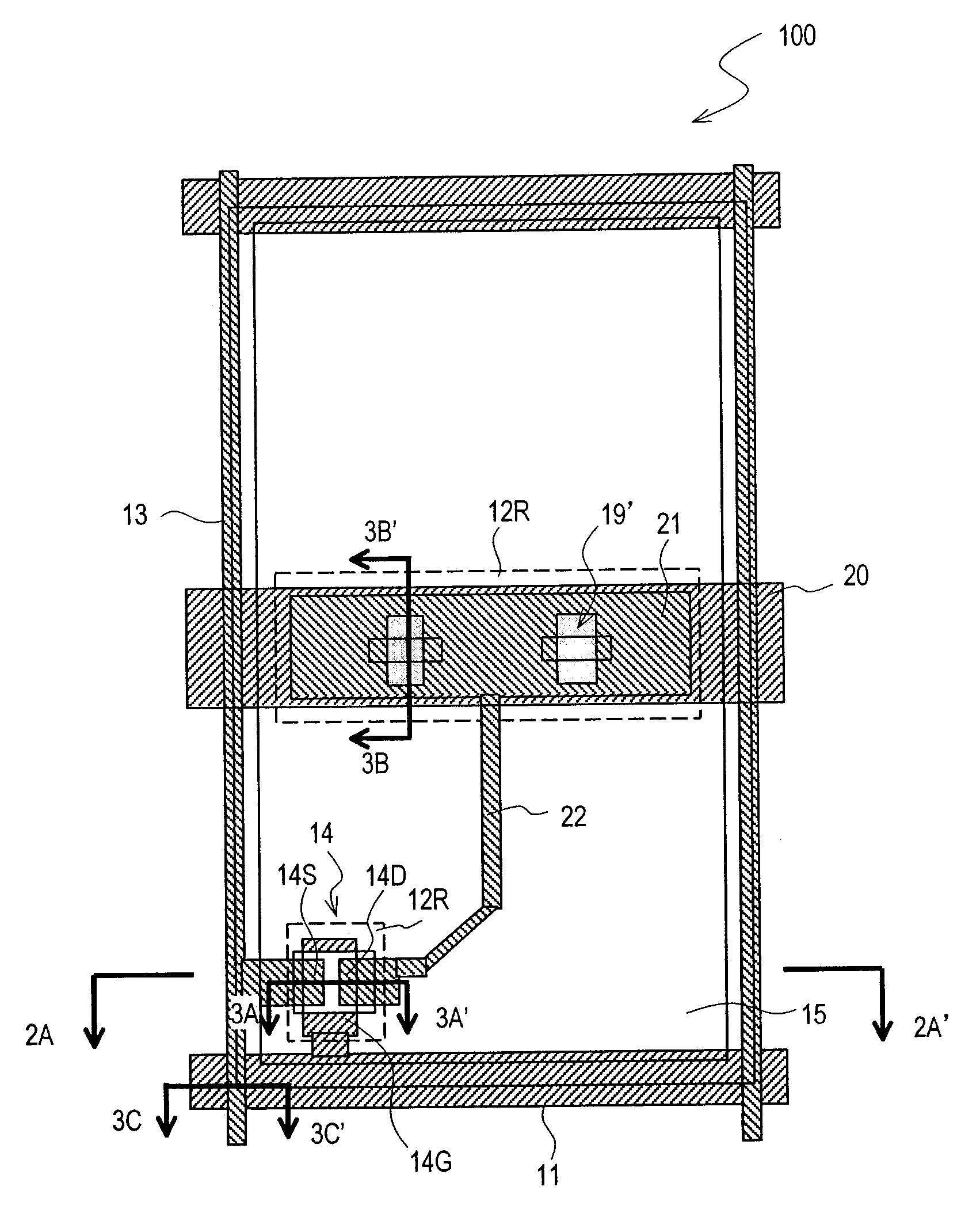
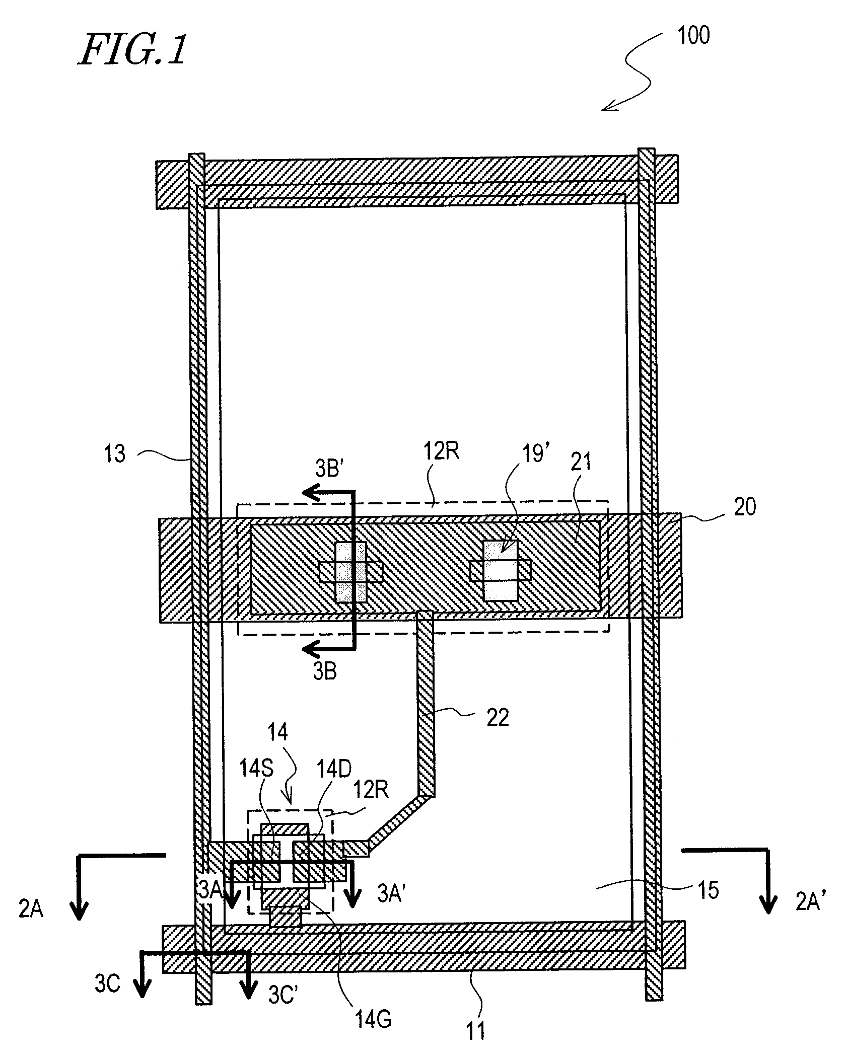
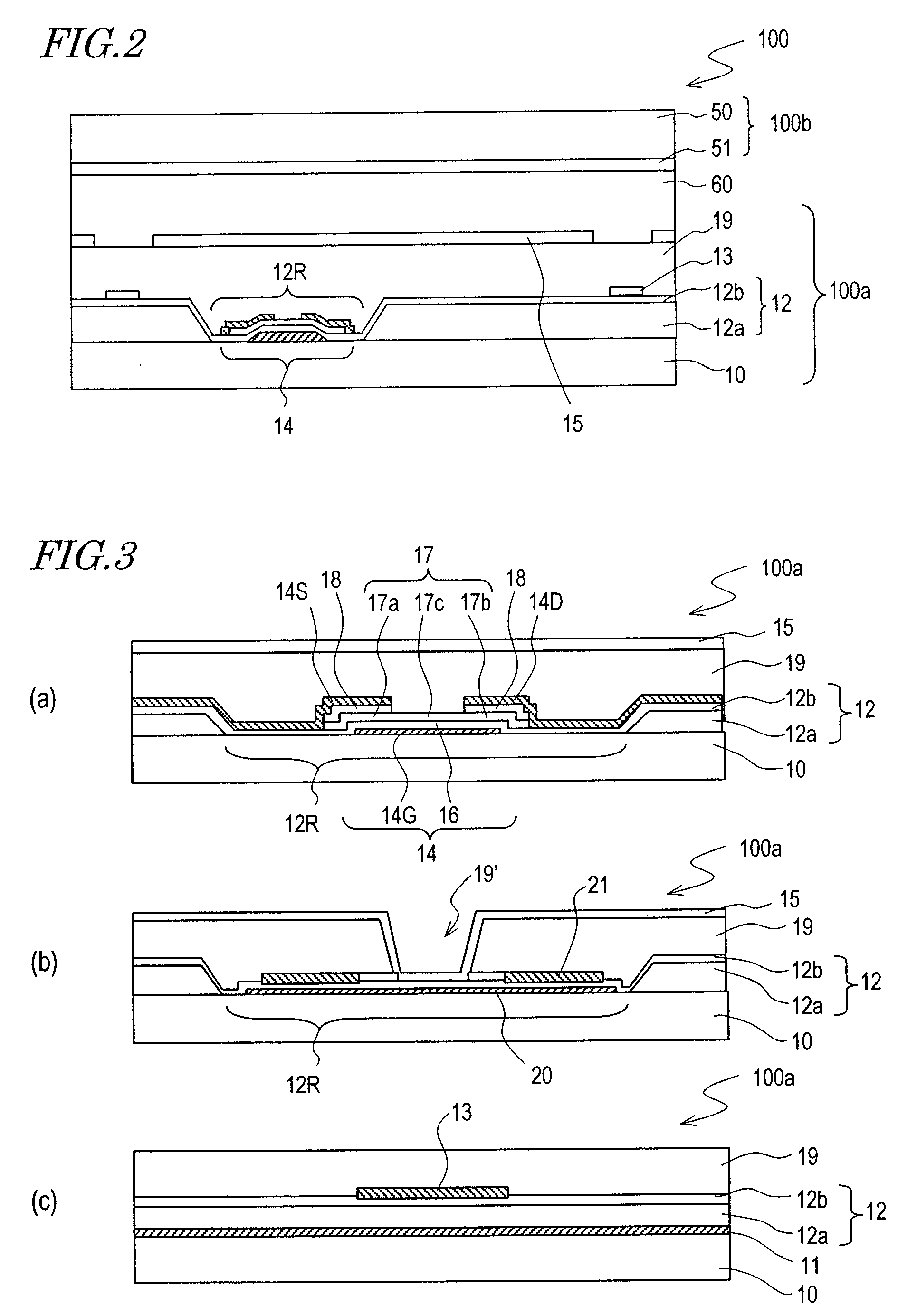
[0087]FIG. 1 and FIG. 2 show a liquid crystal display device 100 according to the present embodiment. FIG. 1 is an upper plan view schematically showing one pixel region of the liquid crystal display device 100. FIG. 2 is a cross-sectional view taken along line 2A-2A′ in FIG. 1.
[0088] The liquid crystaldisplay device 100 includes: an active matrix substrate (hereinafter referred to as a “TFT substrate”) 100a; a counter substrate opposing the TFT substrate 100a (also referred to as a “color filter substrate”) 100b; and a liquid crystal layer 60 interposed therebetween.
[0089] The TFT substrate 100a includes: a transparent insulative substrate (e.g., a glass substrate) 10; a plurality of scanning lines 11 formed on the substrate 10; an insulating film 12 covering the scanning lines 11; and a plurality of signal lines 13 intersecting the scanning lines 11 via the insulating film 12.
[0090] Furthermore, in each pixel region, the TFT substrate 100a includes: a thin film transistor (TFT...
embodiment 2
[0117] With reference to FIG. 6, FIG. 7, and FIGS. 8(a) to (c), a liquid crystal display device 200 according to the present embodiment will be described. Hereinafter, differences from the liquid crystal display device 100 of Embodiment 1 will be mainly described.
[0118] The TFT substrate 200a of the liquid crystal display device 200 differs from the TFT substrate 100a of the liquid crystal display device 100 with respect to the location of the low-stack regions 12R of the multilayer insulating film 12. As shown in FIG. 6, FIG. 7, and FIG. 8(a), the multilayer insulating film 12 of the TFT substrate 200a includes a low-stack region 12R (where the first insulating layer 12a is not formed) in each portion overlapping the channel region 17c. However, the first insulating layer 12a is not removed in all region above the gate electrode 14G, but rather covers edges of the gate electrode 14G. Moreover, as shown in FIG. 6 and FIG. 8(b), the first insulating layer 12a is not removed in all r...
embodiment 3
[0140]FIG. 13 and FIGS. 14(a) to (d) schematically show a liquid crystal display device 300 according to the present embodiment.
[0141] As shown in FIG. 13 and FIGS. 14(a) to (c), the TFT substrate 300a of the liquid crystal display device 300 of the present embodiment has essentially the same construction as that of the TFT substrate 200a of the liquid crystal display device 200 of Embodiment 2.
[0142] However, as shown in FIG. 13 and FIG. 14(d), the TFT substrate 300a of the liquid crystal display device 300 differs from the TFT substrate 200a of the liquid crystal display device 200 in that a plurality of shield electrodes 23 extending substantially in parallel to the signal lines 13 are comprised.
[0143] The shield electrodes 23 of the present embodiment are formed by patterning the same conductive film as that of the scanning lines 11. Each shield electrode 23 is connected to a storage capacitor line 20, and receives a constant potential. Hereinafter, a problem which may occur ...
PUM
Abstract
An active matrix substrate includes a substrate; scanning lines formed on the substrate; an insulating film covering the scanning lines; signal lines intersecting the scanning lines via the insulating film; switching elements formed on the substrate, each operating in response to a signal which is applied to the corresponding scanning line; and pixel electrodes each capable of being electrically connected to the corresponding signal line via the switching elements. The insulating film is a multilayer insulating film including a first insulating layer and a second insulating layer. The first insulating layer is formed of an insulating material containing an organic component, and the multilayer insulating film has a low-stack region in at least a portion of a region overlapping each switching element, the first insulating layer not being formed in the low-stack region. The active matrix substrate reduces the capacitance formed at each intersection between a scanning line and a signal line, without causing an increase in the wiring resistance or a degradation of the driving ability of switching elements.
Description
BACKGROUND OF THE INVENTION [0001] 1. Field of the Invention [0002] The present invention relates to an active matrix substrate which is for use in a liquid crystaltelevision set, a liquid crystal monitor device, a laptop computer, or the like. The present invention also relates to a display device including the active matrix substrate. [0003] 2. Description of the Related Art [0004] Liquid crystal display devices are utilized in various fields because of their thinness and low power consumption. In particular, liquid crystal display devices of an active matrix type, comprising a switching element such as a thin film transistor (referred to as a “TFT”) for each pixel, have a high contrast ratio and excellent response characteristics, and are used in television sets, monitor devices, and laptop computers because of their high performance. The market scale thereof has been increasing in the recent years. [0005] On an active matrix substrate which is used in an active matrix type liqu...
Claims
Application Information
Patent Timeline
Application Date:The date an application was filed.
Publication Date:The date a patent or application was officially published.
First Publication Date:The earliest publication date of a patent with the same application number.
Issue Date:Publication date of the patent grant document.
PCT Entry Date:The Entry date of PCT National Phase.
Estimated Expiry Date:The statutory expiry date of a patent right according to the Patent Law, and it is the longest term of protection that the patent right can achieve without the termination of the patent right due to other reasons(Term extension factor has been taken into account ).
Invalid Date:Actual expiry date is based on effective date or publication date of legal transaction data of invalid patent.

