Method of manufacturing semiconductor device

a manufacturing method and semiconductor technology, applied in the field of manufacturing semiconductor devices, can solve the problems of affecting the film quality of insulation films, the deviation of the design value of semiconductor devices, and the inability to apply techniques to sioch films, so as to avoid the degradation of insulation films

Inactive Publication Date: 2007-11-29
TOKYO ELECTRON LTD
View PDF1 Cites 24 Cited by
  • Summary
  • Abstract
  • Description
  • Claims
  • Application Information

AI Technical Summary

Benefits of technology

[0014] Since the protective film is deposited on the exposed surface of the insulation film formed by the etching process, desorption of the carbon from the insulation film by the succeeding ashing process can be restrained, and thus degrade in film quality of the insulation film can be avoided.

Problems solved by technology

Thus, the reduction in dielectric constant of a film, even in a superficial part thereof, may result in a deviation of properties of a semiconductor device from designed values.
However, since oxidation of the SiOCH film causes desorption of the carbon, this technique cannot be applied to the SiOCH film.
Therefore, this technique also cannot be applied to the SiOCH film.

Method used


Image

  • Method of manufacturing semiconductor device
  • Method of manufacturing semiconductor device
  • Method of manufacturing semiconductor device

Examples


experiment 1

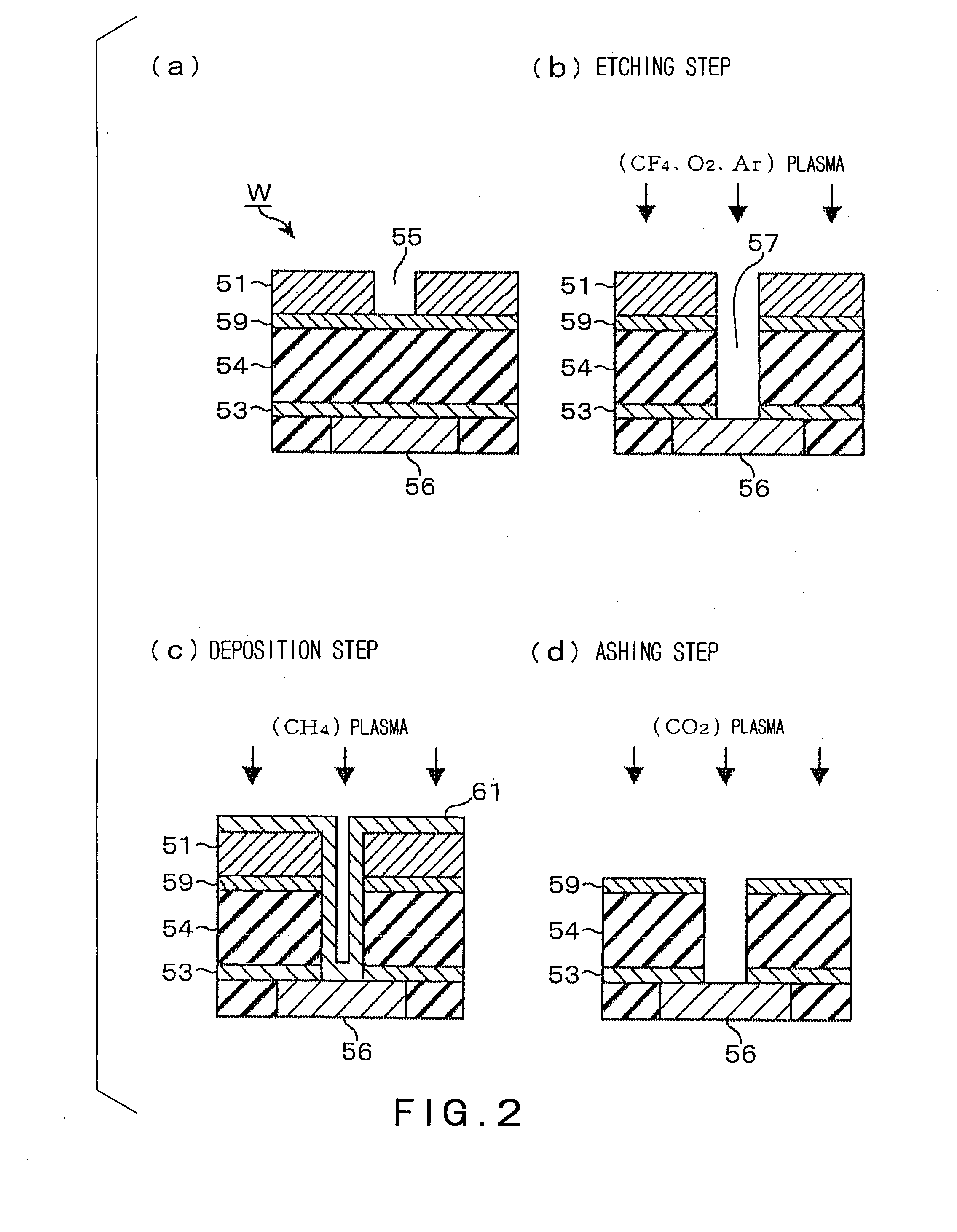
[0076] Comparison of generation of the damage layer 60 between a case in which the protective film 61 is deposited before the ashing step, and a case in which the protective film 61 is not deposited before the ashing step.

example 1

A. Example 1

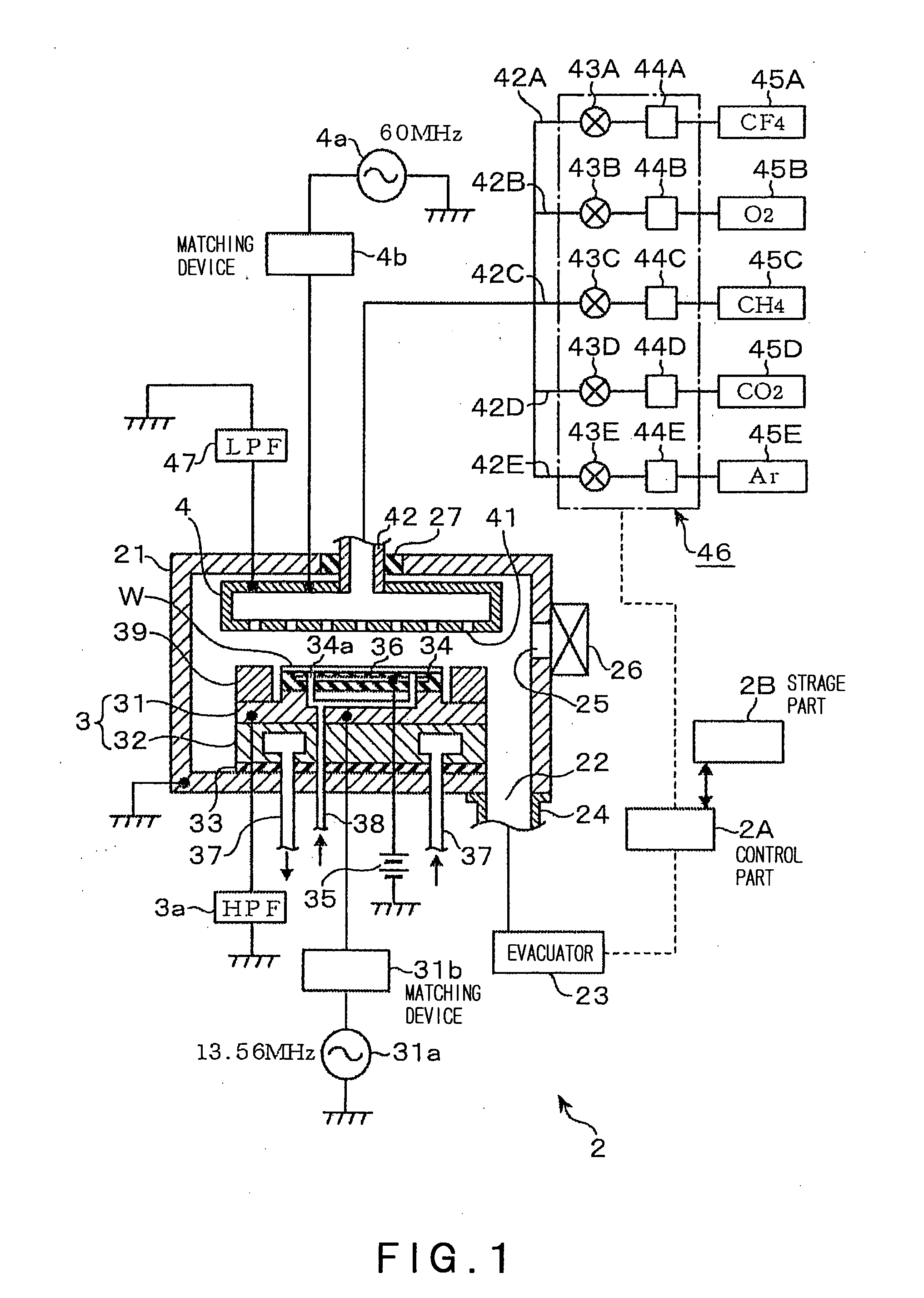
[0077] As described above, after the protective film 61 was deposited on the wafer W shown in FIG. 3, the ashing process was performed. The process conditions in the deposition step of the protective film 61 and the ashing step were as follows:

(Deposition Step)Frequency of upper electrode 460MHzPower of upper electrode 4750WFrequency of lower electrode 3113.56MHzPower of lower electrode 31500WProcess pressure1.3 Pa (10 mTorr)Process gasCH4 / Ar = 100 / 100 sccmProcess period10sec

[0078]

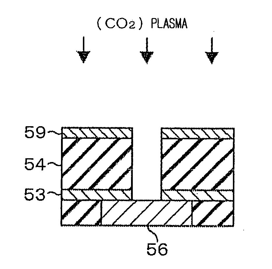
(Ashing Step)Frequency of upper electrode 460MHzPower of upper electrode 4200WFrequency of lower electrode 3113.56MHzPower of lower electrode 31400WProcess pressure20 Pa (150 mTorr)Process gasCO2 = 1500 sccmProcess period60sec

[0079] In order to evaluate an amount of the damage layer 60 of the SiOCH film 54, the thus processed wafer W was immersed in a solution containing 1% by weight of HF for 30 seconds, and then a line width CD2 of the groove 58 was measured. As shown in FIG. 4(a), as compa...

experiment 2

Elemental Analysis

[0088] In order to verify whether the evaluation method of the damage layer 60 in Experiment 1 (immersing the wafer W in a solution containing 1% by weight of HF for 30 seconds, and measuring the ΔCD) is an appropriate evaluation method or not, elements of the wafers W processed in Example 1 and Comparative Example 1-1 were analyzed. By using an electron energy loss spectroscopy (EELS), the elemental analysis was conducted by measuring a position corresponding to a position of the measured line width of the groove 58 in Experiment 1. The results are shown in FIG. 6A and FIG. 6B. In order to show an average composition of the SiOCH film 54, as shown in FIG. 6C, FIG. 6A and FIG. 6B represent an arrangement in which the SiOCH film 54 between the grooves 58 is positioned in a center part thereof, and the wall surfaces of the grooves 58 are positioned on the right and left sides.

[0089] Both in Example 1 and Comparative Example 1-1, there was confirmed on the sidewall ...


PUM

PropertyMeasurementUnit
pressureaaaaaaaaaa
frequenciesaaaaaaaaaa

Abstract

A low dielectric constant film containing a silicon, a carbon, an oxygen, and a hydrogen is formed on a substrate as a semiconductor wafer, and a resist film is formed on the low dielectric constant film. Then, the low dielectric constant film is etched with the use of the resist film as a mask to form an exposed surface of the low dielectric constant film. Next, there is deposited a protective film that covers the exposed surface of the low dielectric constant film formed by etching. Thereafter, by ashing with the use of a plasma containing an oxygen, the protective film and the resist film are removed. During the ashing, desorption of the carbon from an insulation film is restrained by the protective film.

Description

CROSS REFERENCE TO PRIOR APPLICATIONS [0001] This application claims priority from U.S. Provisional Application No. 60 / 781,761 filed on Mar. 14, 2006, and Japanese Patent Application No. 2006-45298 filed on Feb. 22, 2006. The entire contents of these applications are incorporated herein by reference.BACKGROUND OF THE INVENTION [0002] 1. Field of the Invention [0003] The present invention relates to a technique, which is utilized when a semiconductor device is manufactured, for plasma-processing an insulation film of a low dielectric constant film containing a silicon, a carbon, an oxygen, and a hydrogen. [0004] 2. Background Art [0005] In accordance with a recent tendency for a higher degree of integration of a semiconductor device, a pattern to be formed in a substrate such as a semiconductor wafer (referred to as “wafer” below) has to be formed finer. In order to cope with this demand, a resist material and an exposure technique have been improved, and opening dimensions of a resi...

Claims


Application Information

Patent Timeline
Patent Type & Authority Applications(United States)
IPC IPC(8): H01L21/3065C23F1/08
CPCG03F7/40G03F7/427H01L21/76831H01L21/76814H01L21/31138
Inventor NISHIMURA, EIICHIKIHARA, YOSHIHIDEINATA, YASUSHILIN, LYNDON
Owner TOKYO ELECTRON LTD
Why Eureka
Try Eureka