Organic insulating film composition and method of manufacturing organic insulating film having dual thickness using the same

a technology of organic insulating film and composition, which is applied in the direction of organic insulators, solid-state devices, coatings, etc., can solve the problems of reducing the reliability of lcd, deteriorating the properties of tft, and reducing the aperture ratio, so as to increase the aperture ratio, increase the charge mobility, and increase the on-off ratio

Inactive Publication Date: 2007-11-29
SAMSUNG ELECTRONICS CO LTD
View PDF4 Cites 21 Cited by
  • Summary
  • Abstract
  • Description
  • Claims
  • Application Information

AI Technical Summary

Benefits of technology

[0012]Example embodiments provide a TFT including the organic insulating film, which has increased charge mobility, an increased on-off ratio, and an increased aperture ratio and may decrease parasitic capacitance so as to enable the control of a flickering phenomenon.
[0013]Example embodiments provide a display device and an electronic device, each of which may include the TFT, thus increasing reliability and decreasing the manufacturing cost.

Problems solved by technology

When kickback voltage increases, a flickering phenomenon may occur, undesirably decreasing the reliability of the LCD.
However, the properties of the TFT may be deteriorated and the aperture ratio may also be decreased.
Upon the manufacture of the OTFT, the overall manufacturing process may be complicated and the manufacturing cost may be increased, attributed to the additional bank formation process.

Method used


Image

  • Organic insulating film composition and method of manufacturing organic insulating film having dual thickness using the same
  • Organic insulating film composition and method of manufacturing organic insulating film having dual thickness using the same
  • Organic insulating film composition and method of manufacturing organic insulating film having dual thickness using the same

Examples


example 1

Manufacture of Silicon TFT

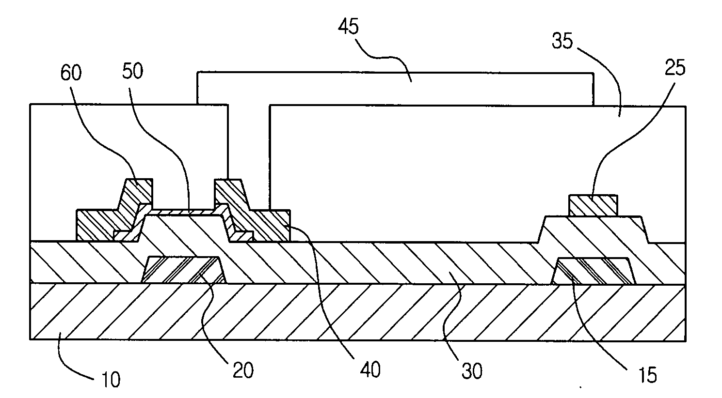
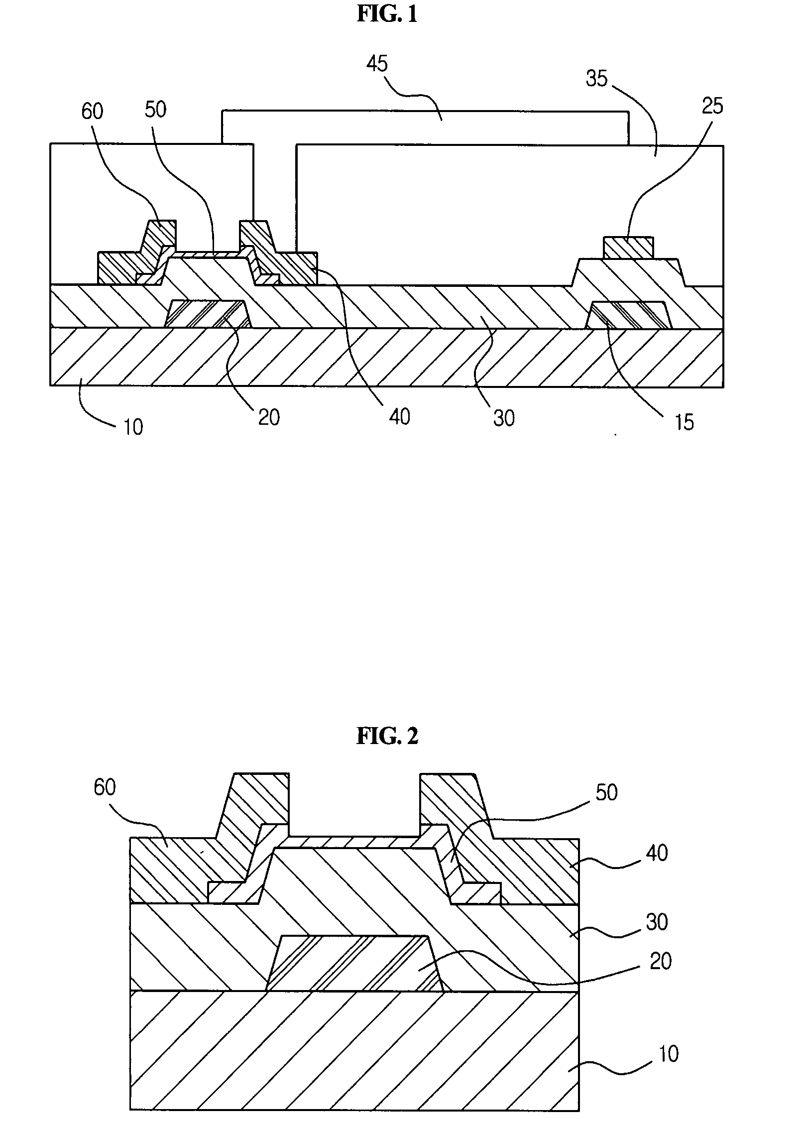
[0069]On a washed glass substrate, a gate electrode having a thickness of about 150 / 3000 / 500 using Mo / Al / Mo was formed, and was then coated with the organic insulating film composition of Preparative Example using a spin coating process at about 2000 rpm to a thickness of about 8,000 . Subsequently, the substrate was soft baked at about 70° C. for about 30 min and then hard baked at about 200° C. for about 1 hour, thus forming an organic insulating film. Thereafter, amorphous silicon and doped amorphous silicon were continuously deposited, after which a channel region was patterned through photolithography and etching. Then, source-drain electrodes were formed, and back channel etching was conducted, thus manufacturing an amorphous silicon TFT having a BCE (Back Channel Etch) structure.

example 2

Manufacture of OTFT

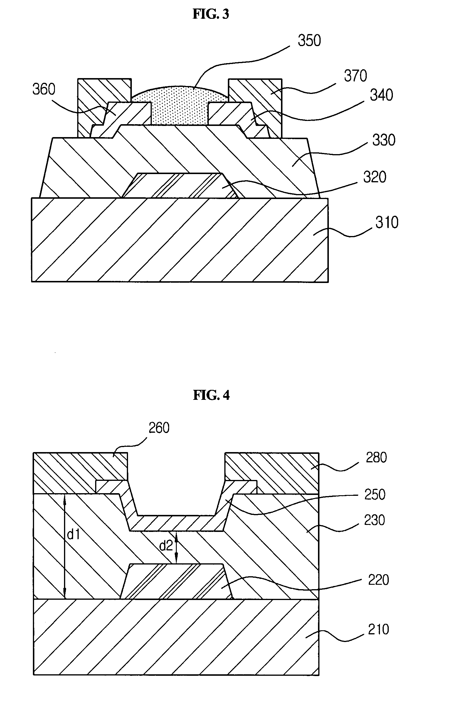
[0070]On a washed glass substrate, a gate electrode having a thickness of about 800 was formed from aluminum, and was then coated with the organic insulating film composition of Preparative Example using a process of spin coating at about 2000 rpm to a thickness of about 8,000 . Subsequently, the substrate was soft baked at about 70° C. for about 30 min and then hard baked at about 200° C. for about 1 hour, thus forming an organic insulating film.

[0071]On the insulating film, Au source / drain electrodes having a channel length of about 100 μm, a channel width of about 1 mm, and a thickness of about 700 were formed, after which a pentacene organic semiconductor layer having a thickness of about 700 Å was formed through thermal evaporation, thereby manufacturing an OTFT having a bottom contact structure shown in FIG. 6. When measuring the transfer properties of the OTFT of example embodiments, the OTFT was confirmed to have electrical mobility of about 0.19 cm2 / Vs ...


PUM

PropertyMeasurementUnit
contact angleaaaaaaaaaa
insulatingaaaaaaaaaa
compositionaaaaaaaaaa

Abstract

Disclosed are an organic insulating film composition for use in the formation of an insulating film having a dual thickness using the hydrophilic / hydrophobic difference between a substrate and a gate electrode, and a method of manufacturing an organic insulating film having a dual thickness using the same. In a display device using a thin film transistor including the organic insulating film of example embodiments, flickering caused by parasitic capacitance may be decreased, and thus reliability may be increased, enabling a simpler manufacturing process and decreased manufacturing cost.

Description

PRIORITY STATEMENT[0001]This non-provisional application claims priority under U.S.C. §119 to Korean Patent Application No. 10-2006-0047761, filed on May 26, 2006, in the Korean Intellectual Property Office (KIPO), the entire contents of which are herein incorporated by reference.BACKGROUND[0002]1. Field[0003]Example embodiments relate to an organic insulating film composition and a method of manufacturing an organic insulating film having a dual thickness using the same. Other example embodiments relate to an organic insulating film composition, suitable for use in forming an insulating film having a dual thickness using the hydrophilic / hydrophobic difference between a substrate and a gate electrode, and to a method of manufacturing an organic insulating film having a dual thickness using the same.[0004]2. Description of the Related Art[0005]In general, a thin film transistor (TFT), which may be formed on a substrate having an increased area, has to date been developed and commerci...

Claims


Application Information

Patent Timeline
Patent Type & Authority Applications(United States)
IPC IPC(8): C08L83/00C08F8/00
CPCC09D183/04C09D183/14H01L29/42384H01L29/4908H01L51/052H01L51/0012C08L2666/04H10K71/191H10K10/471H01B3/18
Inventor SON, KYUNG SEOKHAHN, JUNG SEOKMOON, HYUN SIKLEE, SANG YOONJEONG, EUN JEONG
Owner SAMSUNG ELECTRONICS CO LTD
Why Eureka
Try Eureka