

Semiconductor device having sub-surface trench charge compensation regions and method
a technology of subsurface trenches and capacitor compensation, applied in the direction of semiconductor devices, transistors, electrical apparatus, etc., can solve the problems of increased burden on peripheral control circuits, increased cost of rdson, and significant manufacturing challenges
- Summary
- Abstract
- Description
- Claims
- Application Information
AI Technical Summary
Problems solved by technology
Method used
Image

Examples
Embodiment Construction
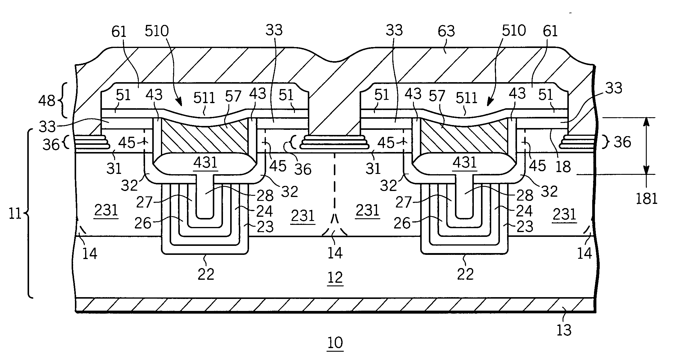
[0014]FIG. 1 shows a partial cross-sectional view of an insulated gate field effect transistor (IGFET), MOSFET, superjunction device, or switching device or cell 10 in accordance with an embodiment of the present invention. By way of example, device 10 is among many such devices integrated with logic and / or other components into a semiconductor chip as part of a power integrated circuit. Alternatively, device 10 is among many such devices integrated together to form a discrete transistor device.
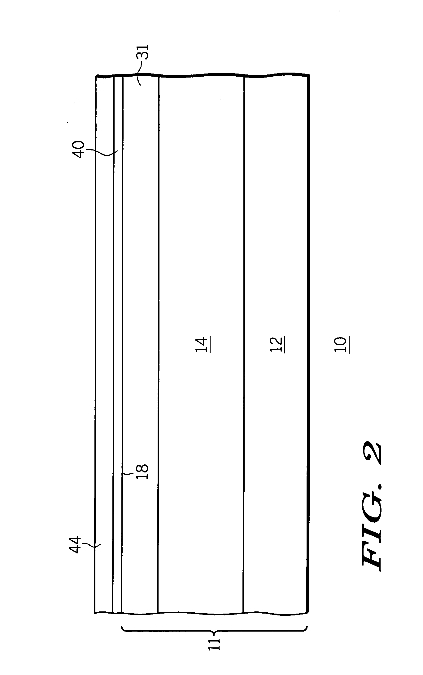
[0015]Device 10 includes a region of semiconductor material 11, which comprises for example, an n-type silicon substrate 12 having a resistivity in range of approximately 0.001 to about 0.005 ohm-cm, and may be doped with arsenic. In the embodiment shown, substrate 12 provides a drain region for device 10, which is coupled to conductive layer 13. A semiconductor layer 14 is formed in or on substrate 12, and in accordance with the present invention is n-type or p-type and doped light enough so...
PUM
 Abstract
Description
Claims
Application Information