Semiconductor device having an improved structure for high withstand voltage
- Summary
- Abstract
- Description
- Claims
- Application Information
AI Technical Summary
Benefits of technology
Problems solved by technology
Method used
Image

Examples
first embodiment
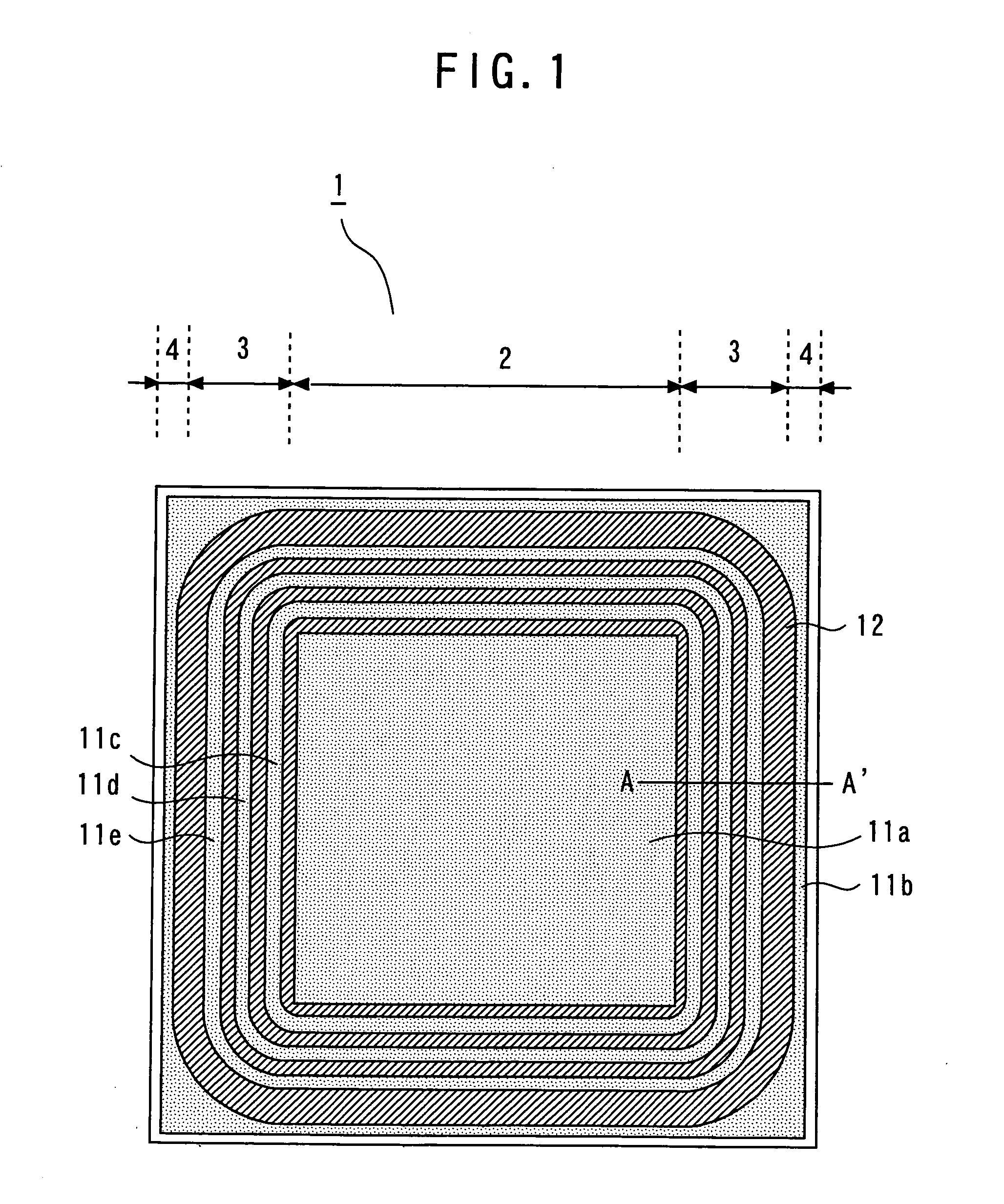
[0019]A semiconductor device according to the first embodiment will be described. FIG. 1 is a plane view viewed from the above of the major surface of a semiconductor chip. On the center portion of the semiconductor chip 1, a device region (active region) 2 is formed. In the exterior of the device region 2, a guard ring region 3 having a plurality of guard rings is formed. Between the guard ring region 3 and the end of the semiconductor chip 1, a channel stopper region 4 is formed. Specifically, on the major surface of the semiconductor chip 1, a guard ring region 3 is formed so as to surround a device region 2, and a channel stopper region 4 is formed so as to surround the guard ring region 3.
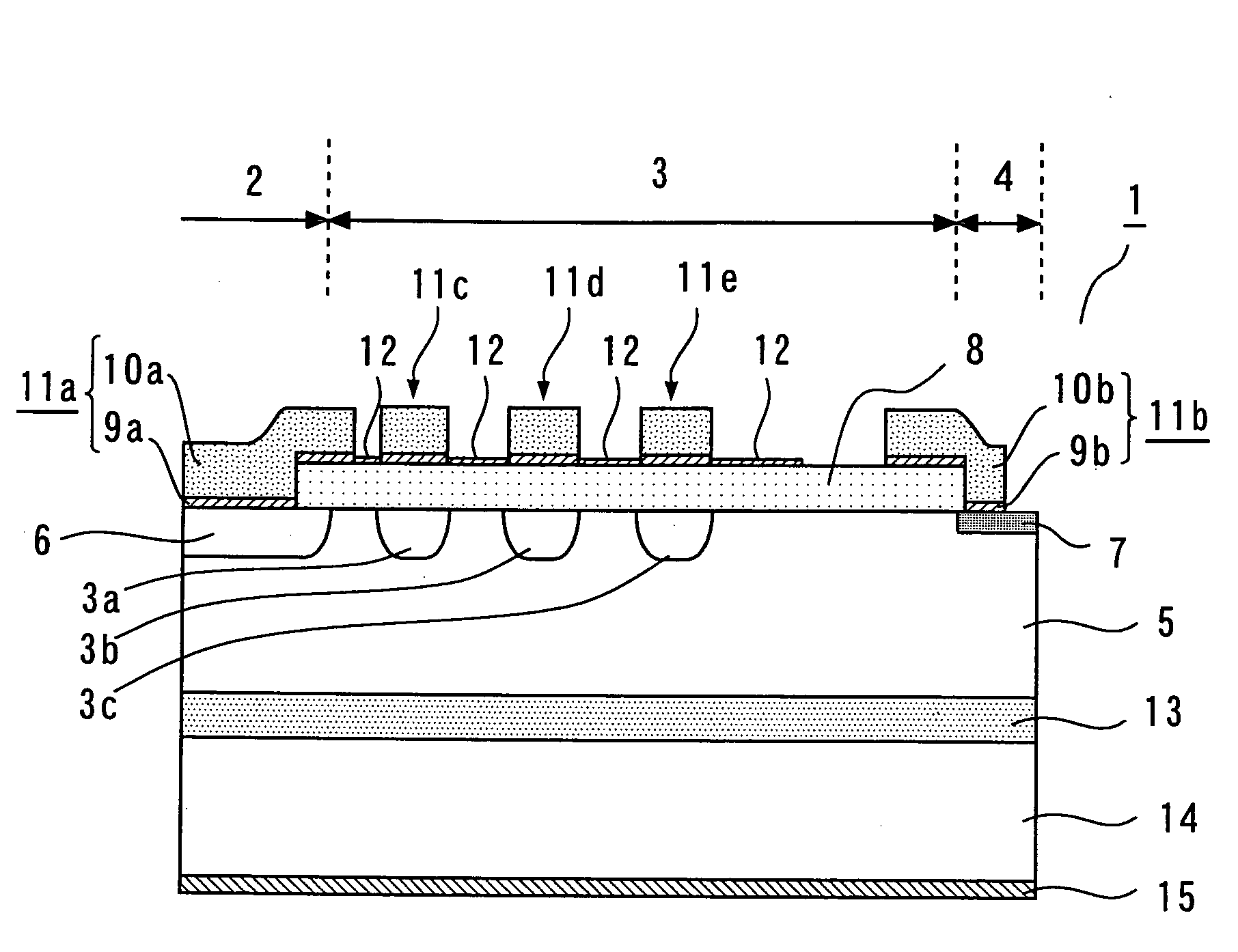
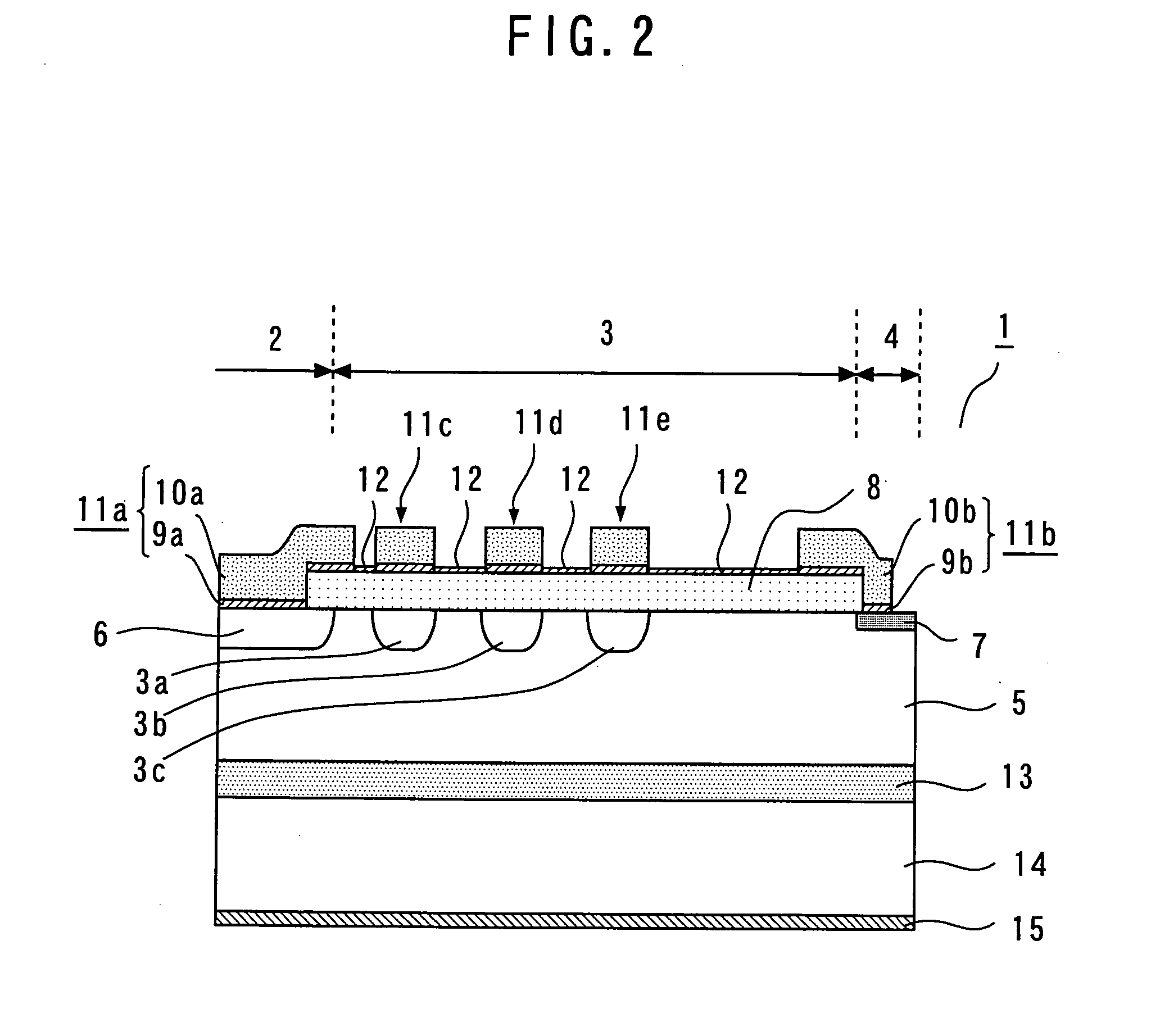
[0020]FIG. 2 shows a sectional view along line A-A′ in FIG. 1. The semiconductor chip 1 is formed using an n-type semiconductor (S1) substrate 5. On the first major surface (upper major surface) of the semiconductor substrate 5, the device region 2, the guard ring region 3, and the channel sto...
second embodiment
[0041]A semiconductor device according to the second embodiment will be described referring to FIG. 3. Here, the description will be focused around different aspects from the first embodiment.
[0042]On an insulating film 8, a conductive film 12 extends from a second surface electrode 11e toward a third surface electrode 11b side, and terminates between the second surface electrode 11e and the third surface electrode 11b. Specifically, on the insulating film 8, the conductive film 12 is confined to extend from the second surface electrode 11e, which is closest to the third surface electrode 11b among three second surface electrodes 11c, 11d and 11e, to a predetermined location between the second surface electrode 11e and the third surface electrode 11b, so as not to be connected to the third surface electrode 11b. Other configurations are identical to those in the first embodiment.
[0043]By the above-described structure, the range where the depletion layer formed when a reverse bias vo...
third embodiment
[0045]A semiconductor device according to the third embodiment will be described referring to FIGS. 4 and 5. Here, the description will be focused around different aspects from the first and second embodiments.
[0046]As FIG. 4 shows, an opening is formed on each of the second diffusion layers 3a, 3b and 3c of the insulating film 8, and a Ti film and an Al film are buried in the opening. By these metal films, the second diffusion layers 3a, 3b and 3c are connected to the second surface electrodes 11c, 11d and 11e, respectively.
[0047]Specifically, conductive connecting portions (contacts) 16a, 16b and 16c are formed on the second diffusion layers 3a, 3b and 3c in the insulating film 8, respectively. By these contacts, the second diffusion layers 3a, 3b and 3c are electrically connected to the second surface electrodes 11c, 11d and 11e, respectively. Other configurations are identical to those in the first embodiment.
[0048]By the above-described structure, the potentials of the second d...
PUM
 Abstract
Description
Claims
Application Information
 - Generate Ideas
- Intellectual Property
- Life Sciences
- Materials
- Tech Scout
- Unparalleled Data Quality
- Higher Quality Content
- 60% Fewer Hallucinations
Browse by: Latest US Patents, China's latest patents, Technical Efficacy Thesaurus, Application Domain, Technology Topic, Popular Technical Reports.
© 2025 PatSnap. All rights reserved.Legal|Privacy policy|Modern Slavery Act Transparency Statement|Sitemap|About US| Contact US: help@patsnap.com