Wafer Scanning Antenna With Integrated Tunable Dielectric Phase Shifters

a phase shifter and scanning antenna technology, applied in the field of antennas, can solve the problems of time-consuming and costly manufacturing of conventional wafer antennas, and the cost of sige and gaas based wafers, and achieve the effects of convenient and cost-effective wafer antenna manufacturing, convenient control, and saving on wafer antenna manufacturing costs

Active Publication Date: 2007-12-06
MERCURY MISSION SYST LLC
View PDF6 Cites 8 Cited by
  • Summary
  • Abstract
  • Description
  • Claims
  • Application Information

AI Technical Summary

Benefits of technology

[0011] The present invention has the advantage that the antenna elements, the phase shifters, RF input / output connection, the RF feed network, and the DC biasing section are all fabricated integrated on the wafer using a thin-film BST process, making the manufacturing of the wafer antenna very convenient and cost-effective, with no need to solder or join discrete components to the wafer antenna. The use of less expensive wafers such as glass or sapphire saves on manufacturing costs for the wafer antenna. The phase shifts in the wafer antenna can be conveniently controlled simply by adjusting the DC bias voltages applied to the BST varactors (capacitors) in the phase shifters coupled to each of the antenna elements on the wafer antenna.

Problems solved by technology

As such, manufacturing such conventional wafer antenna is time intensive and costly.
In addition, SiGe and GaAs based wafers are expensive to manufacture.

Method used


Image

  • Wafer Scanning Antenna With Integrated Tunable Dielectric Phase Shifters
  • Wafer Scanning Antenna With Integrated Tunable Dielectric Phase Shifters
  • Wafer Scanning Antenna With Integrated Tunable Dielectric Phase Shifters

Examples


Embodiment Construction

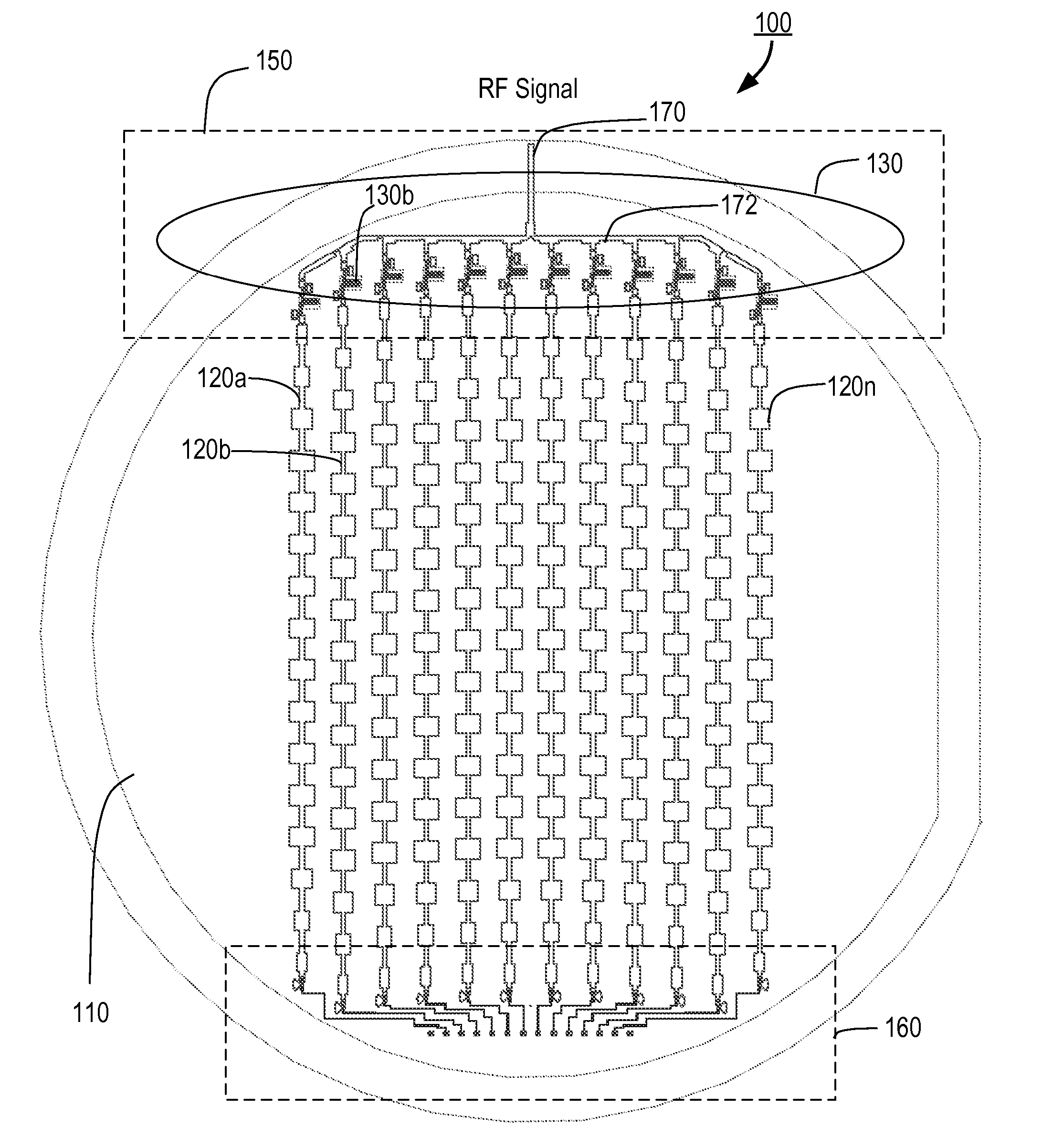
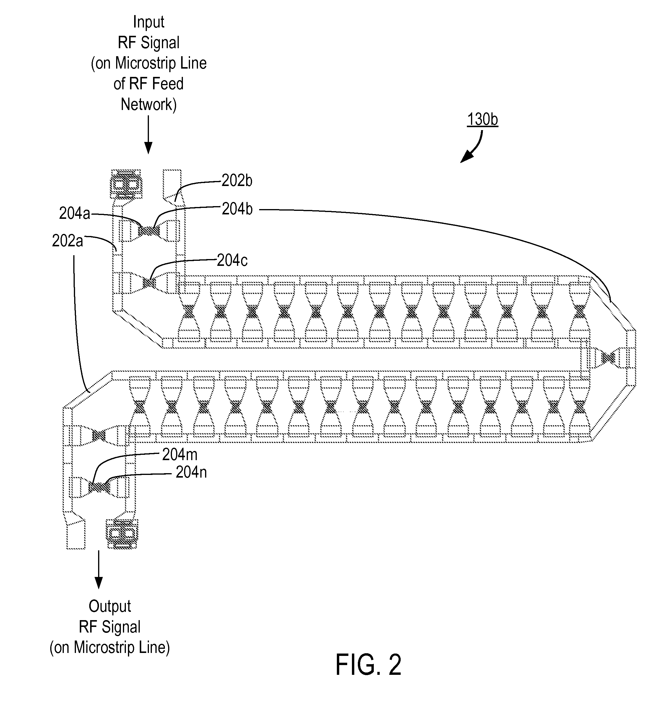
[0022] The Figures (FIG.) and the following description relate to preferred embodiments of the present invention by way of illustration only. It should be noted that from the following discussion, alternative embodiments of the structures and methods disclosed herein will be readily recognized as viable alternatives that may be employed without departing from the principles of the claimed invention.

[0023] Reference will now be made in detail to several embodiments of the present invention(s), examples of which are illustrated in the accompanying figures. It is noted that wherever practicable similar or like reference numbers may be used in the figures and may indicate similar or like functionality. The figures depict embodiments of the present invention for purposes of illustration only. One skilled in the art will readily recognize from the following description that alternative embodiments of the structures and methods illustrated herein may be employed without departing from the...


PUM


Abstract

A wafer antenna comprises a wafer substrate, a plurality of antenna elements integrated on the wafer substrate for radiating and receiving a radio frequency signal, an electrical connection integrated on the wafer substrate; a feed network integrated on the wafer substrate for distributing the RF signal from the electrical connection to the antenna elements and from the antenna elements to the electrical connection, and a plurality of tunable dielectric phase shifters integrated on the wafer substrate with each of the tunable dielectric phase shifters coupled to a corresponding one of the antenna elements and controlling the phase of the RF signal coupled to the corresponding one of the antenna elements.

Description

CROSS-REFERENCE TO RELATED APPLICATION [0001] This applications claims priority under 35 U.S.C. § 119(e) from co-pending U.S. Provisional Patent Application No. 60 / 809,525, entitled “Wafer Antenna with Integrated Barium Strontium Titanate Phase Shifter,” filed on May 30, 2006, which is incorporated by reference herein in its entirety.BACKGROUND OF THE INVENTION [0002] 1. Field of the Invention [0003] The present invention generally relates to the field of antennas, and more specifically, to a wafer based scanning phased-array antenna. [0004] 2. Description of the Related Arts [0005] A conventional wafer antenna is typically fabricated with radiating antenna elements laid out in a fan shape on a silicon germanium (SiGe) or gallium arsenide (GaAs) substrate. Active elements such as phase shifters that couple to the radiating antenna elements are typically soldered or bonded in as discrete components on a circuit board together with the antenna elements built on the SiGe or GaAs substr...

Claims


Application Information

Patent Timeline
Patent Type & Authority Applications(United States)
IPC IPC(8): H01Q1/38H01Q21/00
CPCH01Q3/44H01Q21/065H01Q21/0075
Inventor YORK, ROBERT A.
Owner MERCURY MISSION SYST LLC
Why Eureka
Try Eureka