Liquid crystal display device

a display device and liquid crystal technology, applied in non-linear optics, instruments, optics, etc., can solve the problems of reducing the manufacturing yield rate of tft substrates, affecting the production efficiency of tft substrates, so as to facilitate the repair of short circuits. , the effect of easy cutting

Active Publication Date: 2007-12-06
PANASONIC LIQUID CRYSTAL DISPLAY CO LTD +1
View PDF3 Cites 6 Cited by
  • Summary
  • Abstract
  • Description
  • Claims
  • Application Information

AI Technical Summary

Benefits of technology

[0019]In the liquid crystal display device of the present invention, even when a width (a distance between both edges) of the bus line is large, a portion of the bus line where the opening portion is formed has a width thereof narrowed by an amount corresponding to a width of the opening portion. Accordingly, for example, when a video signal line and the bus line are short-circuited with each other, the bus line can be easily cut at both sides of the intersecting region of the video signal line thus facilitating the repair of the short-circuiting.
[0020]Here, with respect to the opening portion formed in the bus line, by arranging two or more opening portions in parallel in a region sandwiched by two neighboring intersecting regions in the extending direction of the signal lines in the intersecting region, the bus line can be easily cut while maintaining electrical properties of the bus line.

Problems solved by technology

However, there may be a case in which a defect occurs in a step for forming the insulation layer or the semiconductor layer and, for example, the video signal line and the bus line are short-circuited with each other due to the defect.
Accordingly, for example, when the video signal line and the bus line are short-circuited with each other, there has been a drawback that a repair of the short-circuiting is extremely difficult.
Further, because of the difficulty in repairing, there also exists a drawback that a manufacturing yield rate of the TFT substrate is lowered.

Method used


Image

  • Liquid crystal display device
  • Liquid crystal display device
  • Liquid crystal display device

Examples


embodiment

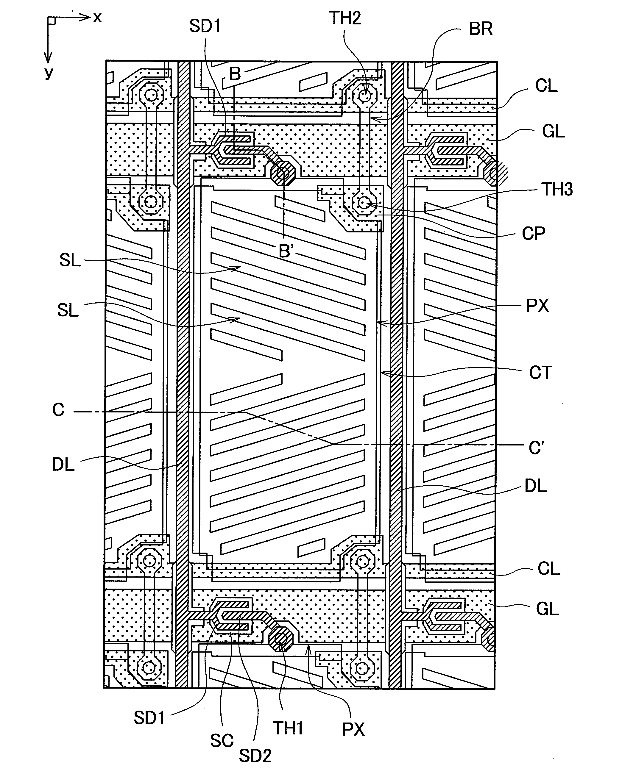
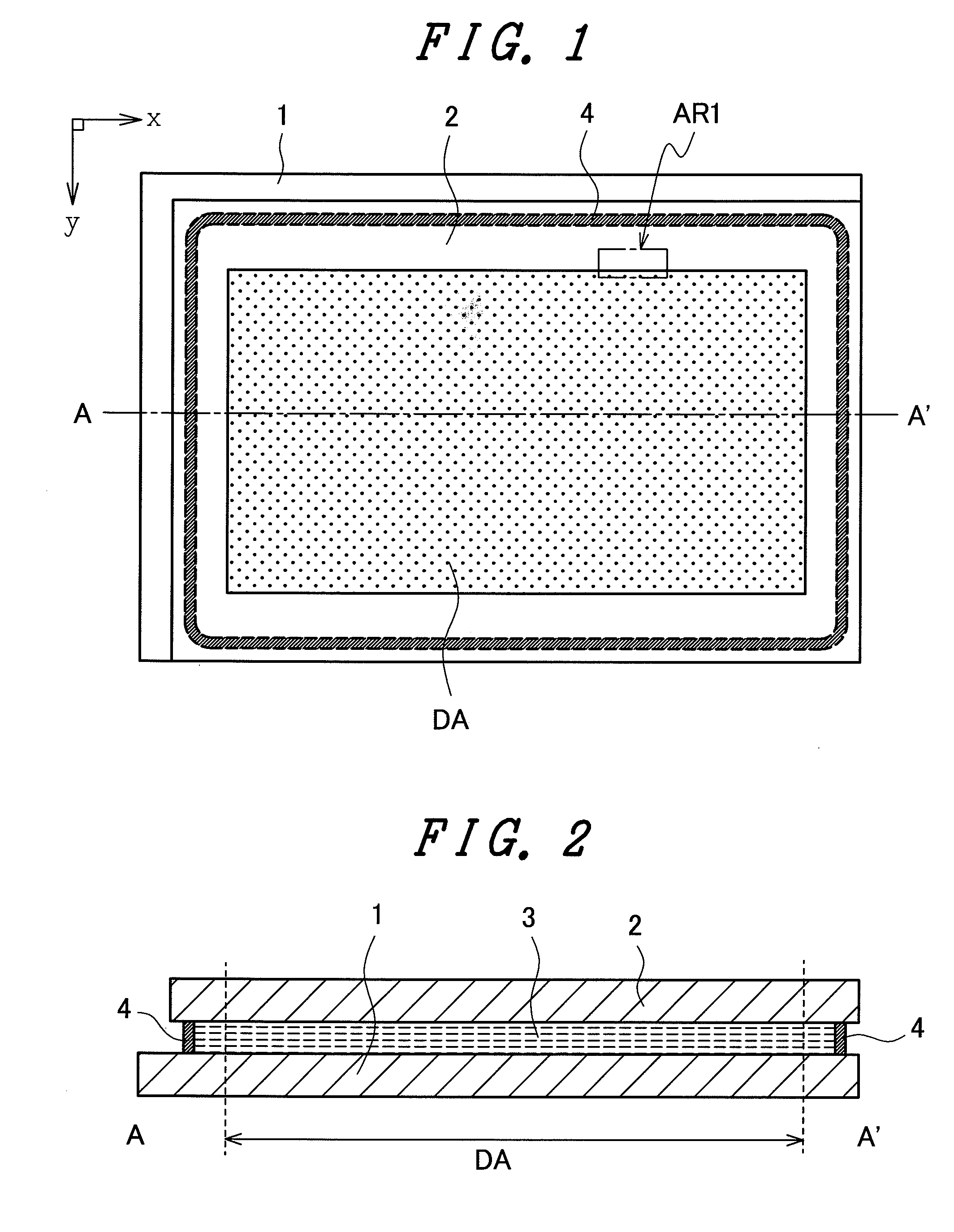
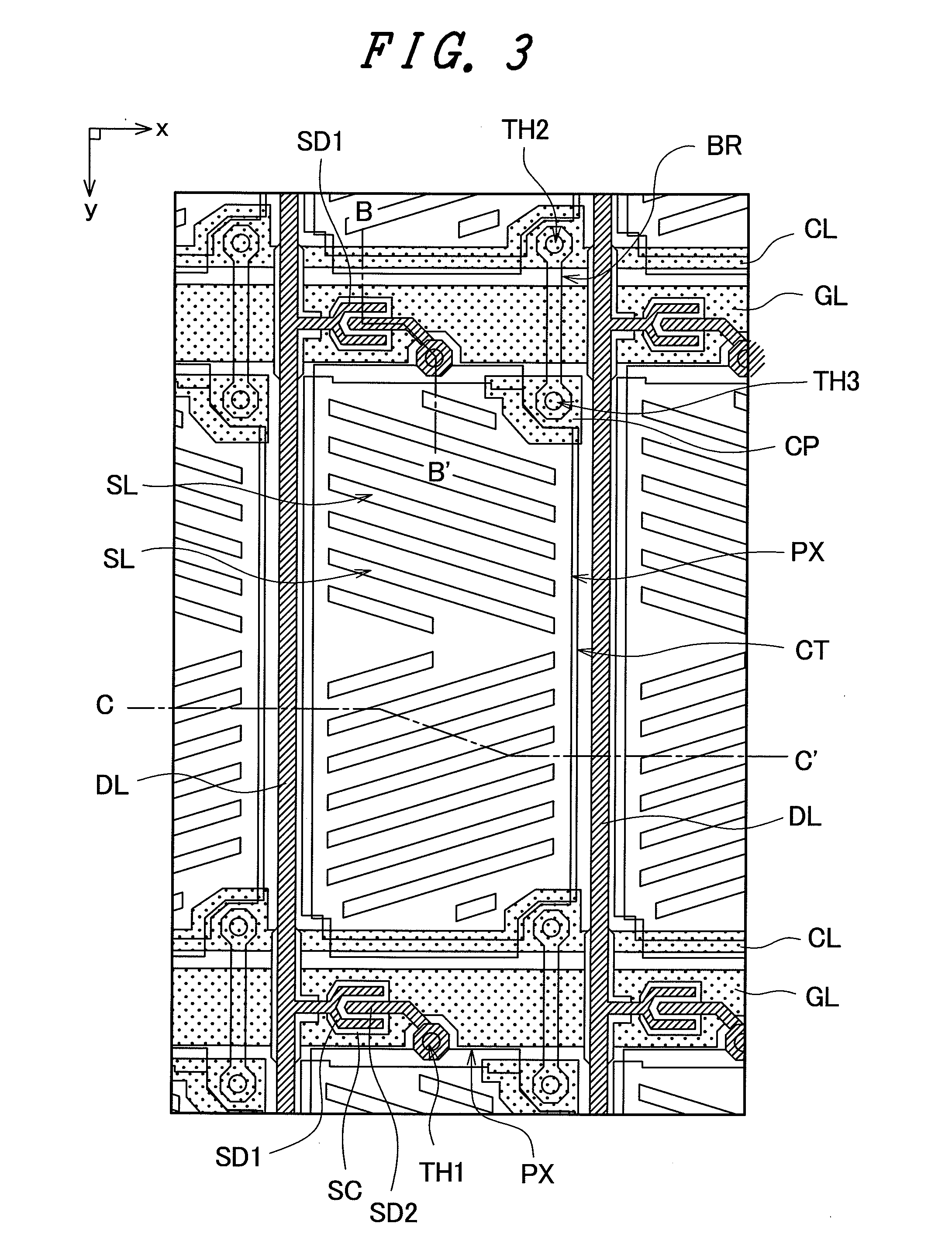
[0038]FIG. 1 and FIG. 2 are schematic views showing the schematic constitution of a liquid crystal display panel of one embodiment according to the present invention.

[0039]FIG. 1 is a schematic plan view of the liquid crystal display panel as viewed from a viewer side. FIG. 2 is a schematic cross-sectional view taken along a line A-A′ in FIG. 1.

[0040]The present invention relates to a display device provided with a display panel having a substrate which forms a bus line outside a display region and on which a plurality of signal lines three-dimensionally intersect the bus line by way of an insulation layer. As one example of such a display panel, a liquid crystal display panel is named. In this embodiment, a lateral electric field drive liquid crystal display panel such as an IPS (In-Plane Switching) liquid crystal display panel is exemplified and the constitution, the manner of operation and advantageous effects of the liquid crystal panel to which the present invention is applied ...


PUM

PropertyMeasurementUnit
conductiveaaaaaaaaaa
shapeaaaaaaaaaa
widthaaaaaaaaaa

Abstract

In a substrate of a liquid crystal display device which forms a bus line which three-dimensionally intersects scanning signal lines, video signal lines and an insulation layer thereon, the present invention facilitates repairs of short-circuiting between the respective signal lines and the bus line. A liquid crystal display device includes a liquid crystal panel which is constituted of a pair of substrates with liquid crystal sandwiched therebetween. Out of the pair of substrates, one substrate includes a bus line which is arranged outside a display region and is electrically connected to a first conductive layer arranged inside the display region, and a plurality of signal lines which three-dimensionally intersect the bus line by way of an insulation layer. The bus line includes opening portions outside intersecting regions where the bus line is overlapped to the signal lines as viewed in a plan view. The opening portions are arranged on both sides of each intersecting region.

Description

[0001]The present application claims priority from Japanese application JP2006-151681 filed on May 31, 2006, the content of which is hereby incorporated by reference into this application.BACKGROUND OF THE INVENTION[0002]1. Field of the invention[0003]The present invention relates to a liquid crystal display device, and more particularly to a technique which is effectively applicable to a liquid crystal display device which arranges a bus line outside a display region.[0004]2. Description of Related Art[0005]Conventionally, a liquid crystal display device has been popularly used as a display for a television receiver set or a personal computer (PC), a display of a mobile phone terminal or a personal digital assistant (PDA) or the like.[0006]The liquid crystal display device is a display device which includes a liquid crystal display panel sealing a liquid crystal material between a pair of substrates. Here, one substrate out of the pair of substrates includes, for example, a plurali...

Claims


Application Information

Patent Timeline
Patent Type & Authority Applications(United States)
IPC IPC(8): G02F1/1343
CPCG02F1/1309G02F1/1343G02F1/1345
Inventor IWATO, HIROAKIICHIHARA, KATSUMI
Owner PANASONIC LIQUID CRYSTAL DISPLAY CO LTD
Why Eureka
Try Eureka