

Integrated Circuit with Debug Support Interface
a technology of integrated circuits and debugging, which is applied in the direction of error detection/correction, fault response, instruments, etc., can solve the problems of increasing the number of integrated circuit package pins on both the development and production parts, and being prohibitively expensive in most cases, so as to achieve the effect of increasing bandwidth
- Summary
- Abstract
- Description
- Claims
- Application Information
AI Technical Summary
Benefits of technology
Problems solved by technology
Method used
Image

Examples
first embodiment
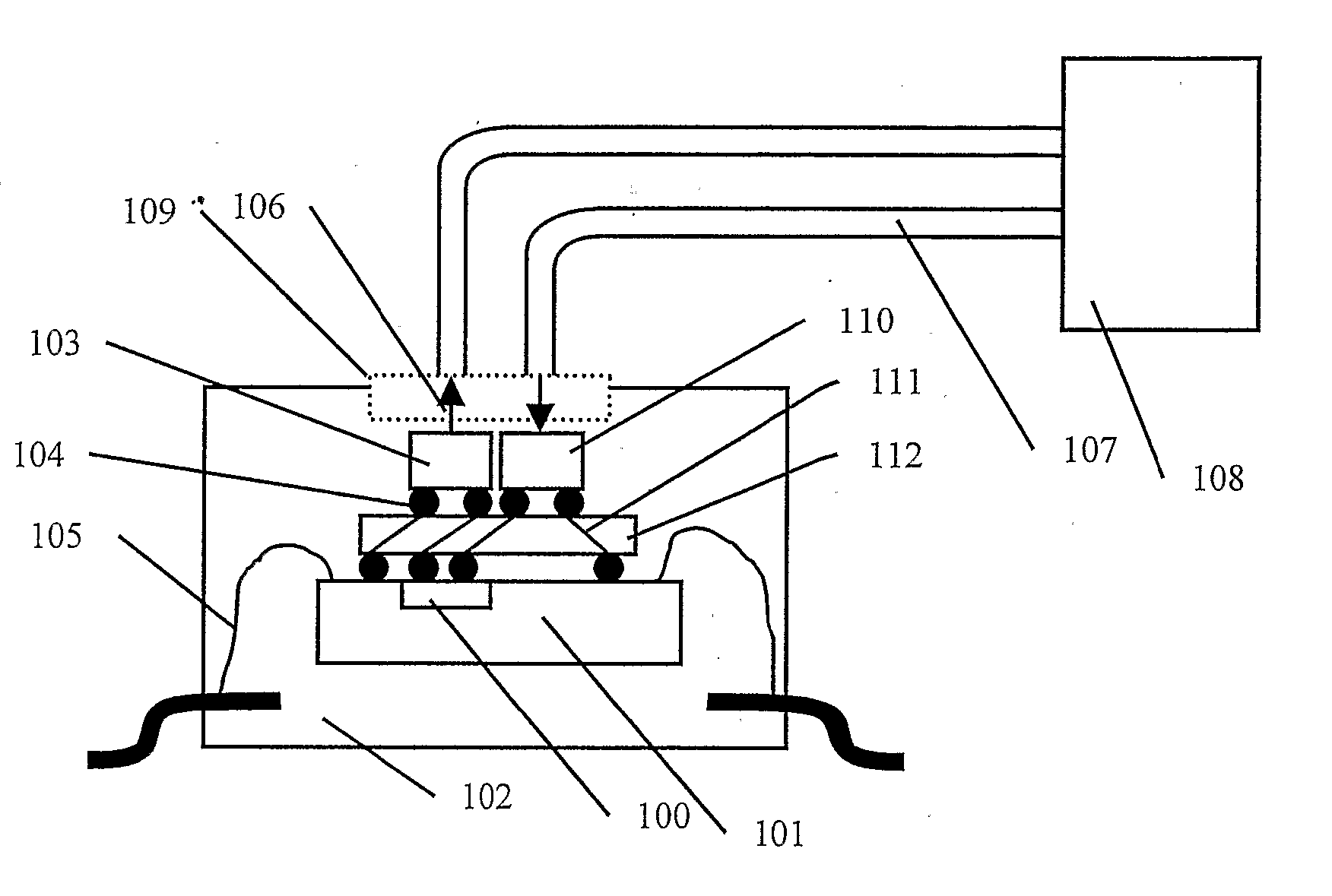
[0053] A first embodiment is shown in FIG. 1 and FIG. 5. Optical sender cells 103 and optical receiver cells 110 are bonded onto the system integrated circuit 101 using a solder bump 104 bonding technique such as flip-chip bonding.
[0054] Thus, electro-optic conversion is provided at the debug support interface. This electro-optic conversion is provided only for the development components. In the mass production components, the arrangement of contact pads may be covered by a passivation layer.
[0055] The electro-optic conversion enables a higher bandwidth transmission link 107 to the external monitoring circuitry 108. For example, a number of electrical signals at the debug interface terminals 104 can be multiplexed together and provided over a shared optical fiber.
[0056] The optical sender cells 103 may be vertical cavity surface emitting lasers, and they may arranged in an array format. The array of lasers may be formed with the optical fiber connections as a sub-assembly, and thi...
second embodiment
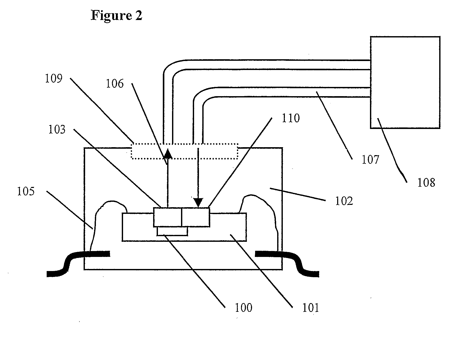
[0060] A second embodiment shown in FIG. 2 has optical sender cells 103 and optical receiver cells 110 integrated into the system integrated circuit 101 to form a monolithic circuit, so that connection to the optical sender cells 103 and receiver cells 110 is made using an integration process.
[0061] In this case, the difference between the mass production components and the development components is that the transmission link 107 is not connected for the mass production components.
third embodiment
[0062] A third embodiment shown in FIG. 3 has a translation mask 112 placed between the optical components 103,110 and the system integrated circuit 101. The translation mask or mask set provides a bonding pad arrangement having an inter pad spacing suitable for the attachment of optical sender cells 103 and optical receiver cells 110 on one side, and a bonding pad arrangement on the other side for the translation mask 112 to be bonded to the system integrated circuit 101. The translation mask 112 contains electrical connections 111 to link the bonding pad means on each side of the translation mask 112.
PUM
 Abstract
Description
Claims
Application Information